
CAM can quote a "low-loss" stack from a marketing datasheet and still miss your impedance and loss budget. The gap is not mysterious SI theory—it is which Dk and Df numbers the fab actually builds to. Dielectric constant (Dk) and dissipation factor (Df) sit on every laminate PDF, but the number buyers paste into a field solver is often the wrong row for the glass style, resin content, thickness, and frequency on the press.
This guide stays on the China fab side of that trap: what Dk and Df control, why marketing tables mislead impedance models, when copper roughness beats chasing the lowest Df, how stability shifts ohms and delay, and which RFQ fields keep impedance quotes honest.
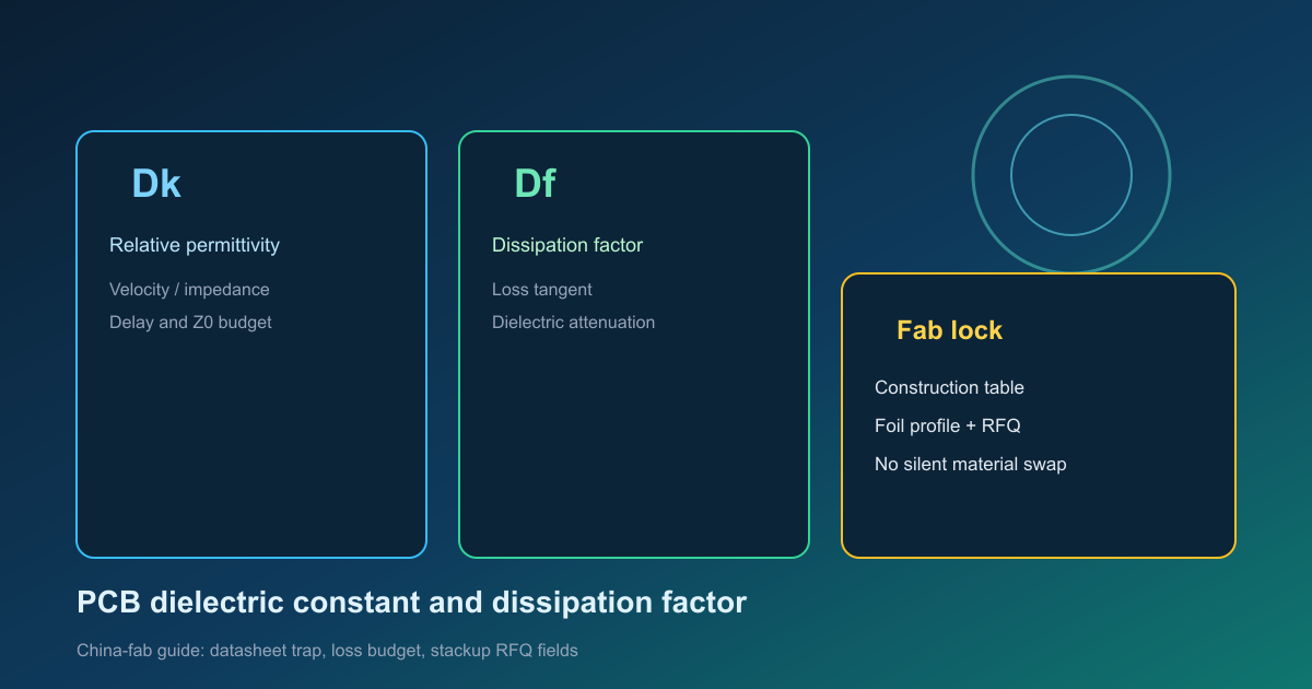
Answer first: what Dk and Df actually control
Dk (dielectric constant / relative permittivity, εr) is the material's ability to store electric energy relative to vacuum. On a PCB it dominates:
- Propagation velocity (and thus delay): as a shop-floor engineering rule of thumb, velocity scales roughly as \(v \propto 1/\sqrt{Dk}\). Higher Dk → slower edge → more delay for the same length.
- Characteristic impedance: for a given geometry and copper, higher effective Dk pulls impedance down. Width and dielectric height still matter—Dk alone does not set Z0—but wrong Dk in the model is the most common "solver said 50 ohm, coupon read 46" story we see in EQ loops.
Df (dissipation factor / loss tangent) describes how much energy the dielectric converts to heat per cycle. Dielectric attenuation rises with frequency and with Df. As a rule of thumb (not an exact SI model), longer channels and higher edge rates feel Df first; short stubs and connector launches often feel copper roughness, vias, and geometry first.
Neither number is a brand badge. They are construction-dependent properties at a stated frequency, resin content, and measurement method. Treat a single "Dk = 3.8 / Df = 0.012" line on a brochure as a screening hint, not a locked stackup input.
💡 Procurement Pro-Tip: Ask the supplier which construction / Dk-Df table (glass style, resin %, thickness, frequency) they will use for impedance calculation—not which marketing PDF they attached to the quote.
The datasheet trap: marketing Dk/Df vs construction tables
Laminate houses publish two very different kinds of numbers. Buyers who mix them get wrong impedance models and apples-to-oranges China quotes.
| Source | What it usually shows | Safe use | Unsafe use |
|---|---|---|---|
| Marketing datasheet | Typical resin %, few frequency points, family averages | Screen FR-4 vs mid-loss vs low-loss families | Paste into field solver as exact stack Dk/Df |
| Fabricator construction / Dk-Df table | Glass style, resin content, ply thickness, frequency of measurement | Impedance model, CAM EQ, RFQ lock | Ignoring frequency and glass style when quoting Z0 |
| In-house fab process sheet | What that plant actually presses and models | Production stack agreement | Assuming every China fab uses the same row for the same brand |
Marketing sheets optimize readability. Construction tables optimize press and SI reality. Same laminate family can move effective Dk several tenths when you change from a resin-rich thin prepreg to a glass-heavy core, or when you read 1 GHz vs 10 GHz data. If purchasing locks "Brand X equivalent" from a one-line Dk while engineering modeled a specific construction row, the lot can pass TDR on the fab's model and still miss your SI budget.
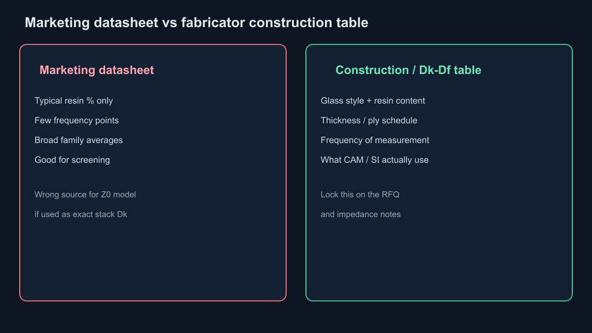
⚠️ Watch Out for: Quotes that say "meets datasheet Dk" without naming the construction table row and reference frequency. That phrase is not an impedance contract.
For coupon/TDR lot evidence and geometry authority, use the deeper shop-floor guide on controlled impedance custom PCBs—this article stops at the material numbers that feed that table.
Rough formulas buyers can use without pretending they are solvers
Keep these labeled as engineering rules of thumb, not replacements for a 2D/3D field solver or fab process model:
- Velocity / delay: \(v \approx c / \sqrt{Dk_{eff}}\). A jump from Dk_eff 3.6 to 4.0 is a few percent more delay on the same length—enough to matter on matched SerDes or RF delay lines, often invisible on short GPIO.
- Impedance direction: holding geometry fixed, higher Dk → lower Z0; lower Dk → higher Z0. Fab recovery is usually width/spacing or dielectric height—not hoping Df changes Z0.
- Dielectric loss trend: dielectric attenuation rises as frequency and Df rise. Doubling frequency roughly doubles the dielectric contribution in simple loss-tangent models; copper loss has its own skin-effect curve.
- Total channel loss ≠ Df alone. Foil roughness, etch factor, via stubs, and connector launches can dominate on short-to-mid channels even when Df looks excellent on paper.
If your team needs 5G front-end material selection detail (PTFE-ceramic vs hydrocarbon, hybrid RF stacks), see 5G RF front-end PCB materials. This piece stays on Dk/Df literacy for general high-speed and RFQ honesty.
Copper roughness can beat the lowest-Df laminate
Buying the lowest Df core while leaving standard foil on long outer microstrips is a common cost leak. At multi-gigabit rates, foil profile (STD, RTF, VLP, HVLP-class) changes conductor loss through roughness. On short channels, upgrading foil and cleaning via stubs often buys more margin per dollar than jumping an entire mid-loss stack to ultra-low-loss resin.
Practical factory view:
- Short digital / modest edge rate: standard FR-4 family + controlled geometry often wins; obsessing over Df 0.004 vs 0.008 rarely pays.
- Mid-length SerDes: mid-loss or low-loss resin and a named foil profile usually beat "lowest Df, any foil."
- Long backplane / high loss budget pressure: low-loss or ultra-low-loss families (e.g. Megtron-class examples) plus smooth foil and hybrid stack discipline.
- Microwave / RF critical: PTFE-ceramic or other RF grades as industry material examples—still lock construction tables and foil, not brochure headlines.
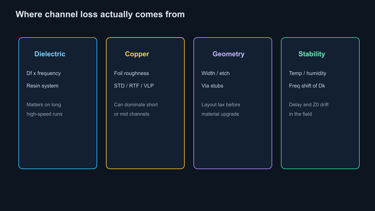
💡 Procurement Pro-Tip: Put foil type next to laminate grade on the RFQ. A silent STD-foil substitution on a VLP-modeled stack is a loss-budget change, not a paperwork nicety.
Copper foil selection detail lives in copper foil HTE and low-roughness PCB and the broader copper foil for PCBs notes—link them when roughness is the deciding lever.
Stability: frequency, temperature, and moisture move Dk/Df
Datasheet Dk at one lab condition is not the Dk your board sees in a humid field rack.
- Frequency: many resin systems show Dk and Df shifting across MHz→GHz. Model and coupon reference frequency should match the interface you care about—or at least be stated so CAM and SI are not arguing past each other.
- Temperature: Dk and Df drift with temperature; impedance and delay drift with them. Automotive and outdoor enclosures feel this more than lab benches.
- Moisture: some resin systems absorb humidity; effective Dk can rise and loss can worsen after bake-out windows close. Moisture-sensitive builds need bake, storage, and sometimes material family choices that purchase forgot to price.
Stability is why "same brand, any construction" fails audits. A humidity-shifted Dk moves Z0 and length-match assumptions even when etch was perfect.
Practical selection ladder: FR-4 → mid-loss → low-loss → ultra-low-loss
Prefer generic families first; name well-known grades only as industry examples, not as ads.
| Family (generic) | Typical buyer trigger | What to lock beyond "low loss" |
|---|---|---|
| Standard FR-4 / high-Tg FR-4 | Cost, short nets, low-GHz, non-critical loss | Tg, glass style if impedance-critical, no silent swap |
| Mid-loss | Moderate length, mixed digital, tighter loss than FR-4 | Construction table row, foil, impedance table |
| Low-loss (e.g. Megtron-class examples) | Long SerDes, backplane-ish loss budgets | Exact grade or AVL alternates, foil profile, hybrid yes/no |
| Ultra-low-loss / RF (e.g. PTFE-ceramic industry grades) | Microwave, antenna feeds, very tight loss | Hybrid press plan, Dk table frequency, special process notes |
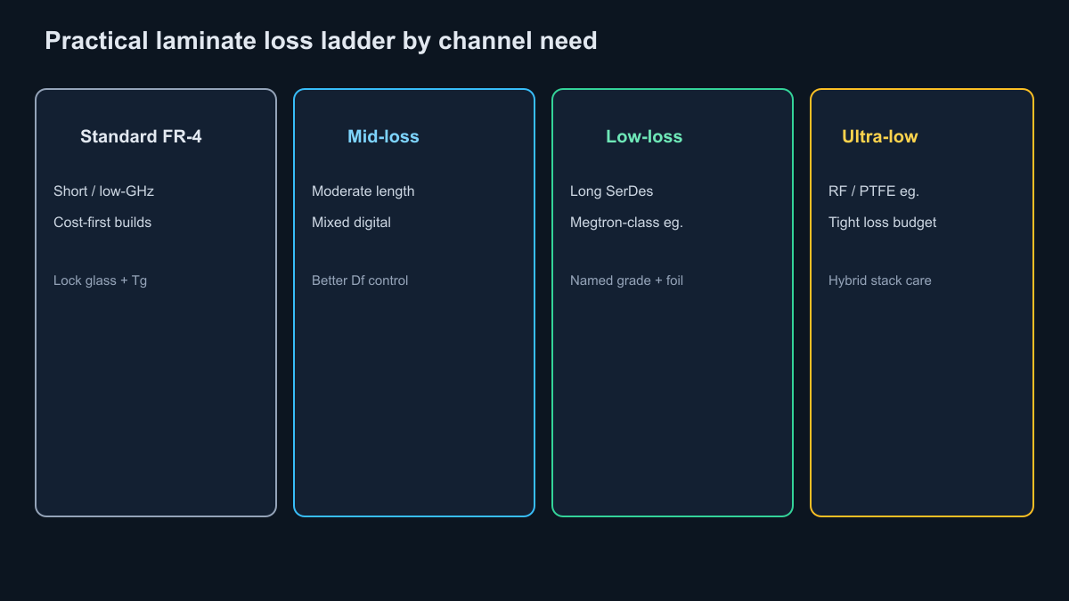
Do not jump two rungs because a competitor brochure looked greener. Jump when the loss budget and length say the cheaper family cannot close—and when foil/geometry upgrades are already on the table.
Stackup construction language (cores, prepregs, press-out) pairs with multilayer PCB stackup fabrication.
China fab RFQ matrix: fields that keep impedance quotes honest
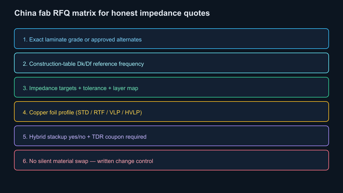
Paste this checklist into the fab drawing or RFQ cover sheet. Incomplete rows are how two "50 ohm low-loss" quotes diverge by several ohms and several dB.
| RFQ field | What good looks like | Failure mode if missing |
|---|---|---|
| Laminate grade | Exact grade or written approved alternates | Silent "equivalent" swap mid-lot |
| Construction / Dk-Df reference | Table ID + glass/resin/thickness + frequency | Marketing Dk used as model |
| Impedance targets | Ohms, tolerance, layer/reference map | Geometry invented per CAM |
| Copper foil profile | STD / RTF / VLP / HVLP-class as required | Rough foil on a smooth-foil model |
| Hybrid stackup | Yes/no; which layers are which family | Press and Dk mix surprises |
| TDR / coupon | Required or waived in writing | "We modeled it" without lot evidence |
| Change control | No silent material swap; ECO path | Purchasing-friendly substitutions |
⚠️ Watch Out for: "Same Dk family" substitutions. Effective Dk for your glass style and resin content can move enough to fail a ±10% coupon even when the brochure family name looks identical.
Close the material note before you argue about mils
A clean Dk/Df conversation on a China RFQ sounds boring on purpose: named grade or AVL list, construction-table frequency, impedance table filled, foil profile stated, hybrid called out, coupon/TDR scoped, and written ban on silent swaps. What gets expensive is the opposite—marketing Dk in the solver, STD foil on a VLP model, and three fabs each inventing a different "equivalent."
XFPCB reviews stackup and impedance packages the way CAM does on the floor: construction numbers first, then geometry authority and lot evidence. Share your stackup draft, impedance targets, and whether foil/laminate may substitute under written approval—we will return a DFM read on whether the Dk/Df lock matches the board you intend to ship.
Related XFPCB guides
- Controlled impedance custom PCBs — impedance tables, geometry authority, coupons/TDR
- 5G RF front-end PCB materials — RF material families for front-end work
- Multilayer PCB stackup fabrication guide — cores, prepreg, press construction
- Copper foil HTE and low-roughness PCB — foil profile vs conductor loss