
The EMI chamber failed a board that had already passed schematic review, DRC, and a tidy BOM. Return-current loops were long because the layer order was frozen late, after placement and escape routing had already burned the copper budget. The same panel also bowed enough after reflow that fine-pitch connectors sat off the seating plane. Neither failure lived in the netlist. Both lived in a stackup treated as an afterthought instead of a manufacturing contract.
Engineers and buyers who lock layer count in the last week of layout keep fighting the same China-fab loop: CAM engineering questions on dielectric thickness, impedance coupons that do not match the drawing, and yield hits from asymmetric copper or too many lamination cycles. This guide stays on that broader multilayer problem -- 4 through 12+ layers -- and the fab language that keeps RFQs honest.
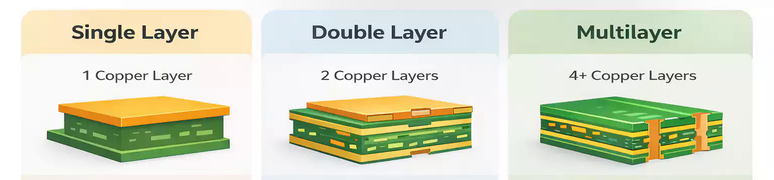
What a multilayer board actually is
A multilayer PCB is a pressed sandwich of copper foils and dielectric sheets. Outer copper typically carries pads and short breaks; inner copper carries signals, power, and ground. Between copper sheets sit cores (already bonded copper-clad laminate) and prepreg (uncured resin-glass that flows and bonds during press). Heat and pressure fuse that stack into one rigid board. The dielectric thicknesses and copper weights are not decoration -- they set impedance, loss, crosstalk, and how much the panel wants to warp when resin shrinks.
That sandwich is different from a double-sided board in kind, not only in count. Two-layer work has no buried copper; every interlayer jump is a full-thickness plated through-hole. Multilayer work adds internal planes and signal layers that only exist after inner imaging, etch, and lamination. Routing density rises, return paths can sit next to continuous copper, and EMI behavior becomes something you can plan instead of hoping pours will finish the job.
Industry planning notes often put roughly half of common signal-integrity, power-integrity, and EMI field failures back to weak stackup choices. Planning the build before dense layout is not a CAD luxury. It is how you avoid discovering that the BGA needs an extra plane or a laser microvia cycle after the outline is frozen.
Choose layer count from BGA, rails, and speed -- not habit
Layer count should follow density, power distribution, and edge rates. Habit ("we always do six") and fear ("twelve looks safer") both waste money or burn schedule.
A practical China-fab reading of the same problem looks like this:
- Four layers: many MCU, IoT, and industrial I/O boards when one solid ground and one power (or dual ground) plane can carry return and PDN needs.
- Six layers: denser digital routing, mixed-signal partitions, or moderate-speed interfaces that need cleaner references without jumping to HDI.
- Eight layers: USB 3.x, PCIe, DDR-class links, and boards that need dedicated signal pairs with adjacent planes on both sides of critical routes.
- Ten to twelve-plus layers: multiple BGAs, many power rails, controlled impedance across several interfaces, and EMC budgets that punish fragmented returns.
Count power rails and the largest BGA before you count "nice to have" signal layers. Pin pitch and I/O count drive escape layers; each additional controlled-impedance interface wants a predictable reference. Even layer counts press more evenly than odd counts, so most production menus stay even unless a specialty construction forces otherwise. High-density packages can force thinner dielectrics and HDI -- those choices change cost more than adding one casual signal layer on a standard through-hole menu.
Freeze construction with the fab while the schematic is still movable. Changing from a stocked six-layer menu to a custom eight-layer hybrid after placement is how warpage and impedance EQs start.
Via types that change fab cost
Vias are not free connectors. Each type changes drill method, plating, and how many times the panel must be pressed.
Through-hole vias (PTH) drill the finished board from top to bottom after lamination. They are the lowest-cost interconnect for general routing and component leads. They also consume routing real estate on every layer they pierce, which hurts under dense BGAs.
Blind vias connect an outer layer to one or more inner layers without punching the full stack. Buried vias connect only internal layers. Both need sequential build steps: cores are drilled and plated before final press, or laser microvias are formed on build-up layers. Every extra sub-lamination cycle adds thermal stress, registration risk, and price.
HDI microvias (laser-drilled, small aspect ratio) support fine-pitch breakout and short stubs, but each HDI build-up layer is another press. Crossing blind and buried structures that force overlapping sub-laminations are a common cost trap; merging overlapping vias into fewer cycles is often the manufacturable fix. Aspect ratio limits still apply: mechanical drills tolerate thicker stacks; laser microvias need thin outer dielectrics.
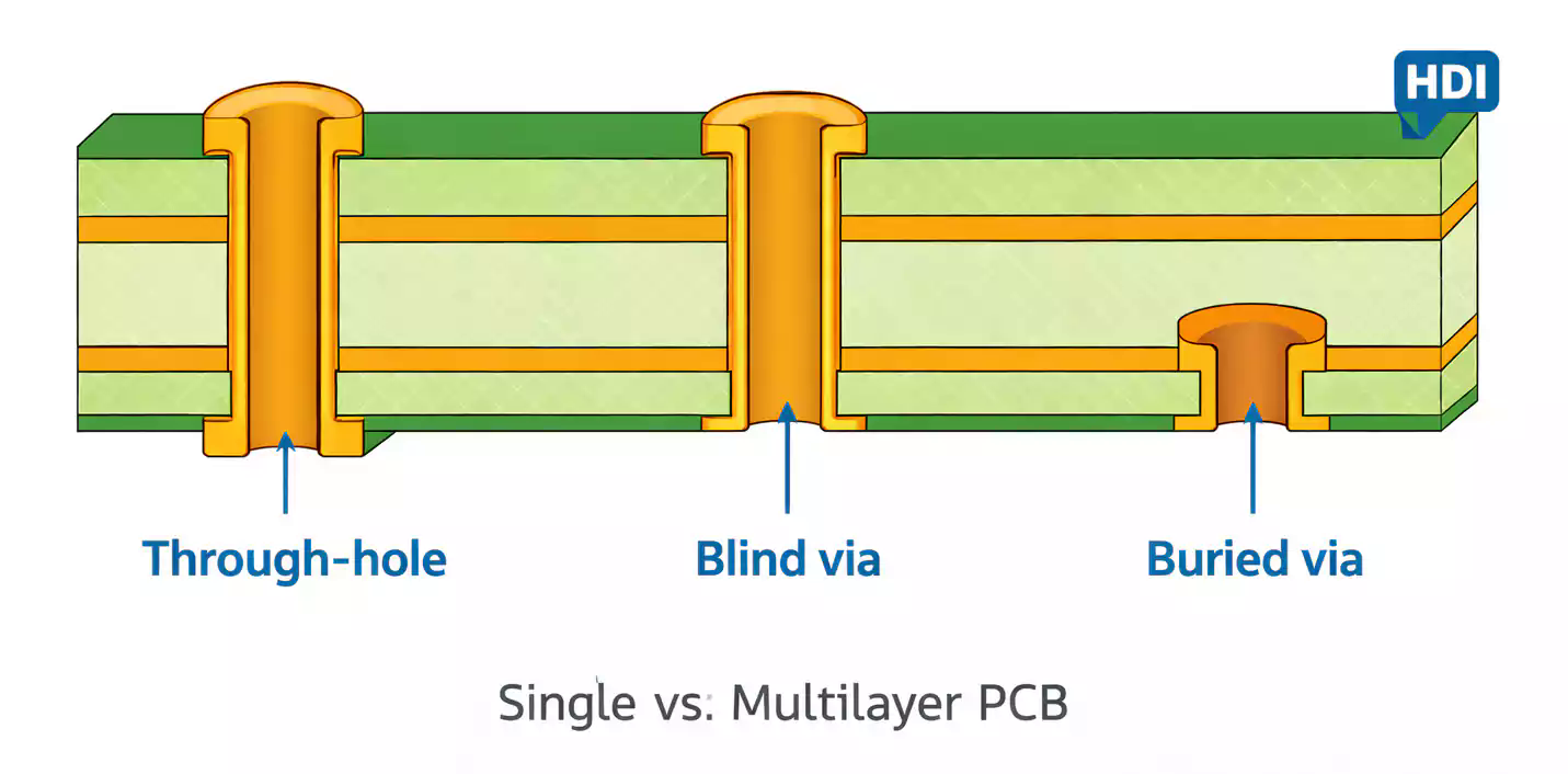
State via technology on the RFQ the same day you state layer count. "Blind/buried TBD" is how quotes diverge and how CAM later asks for a redesign.
Stackup rules that read as fab constraints
Three rules show up again and again in field failures, and they map cleanly to what a press and etch line can hold.
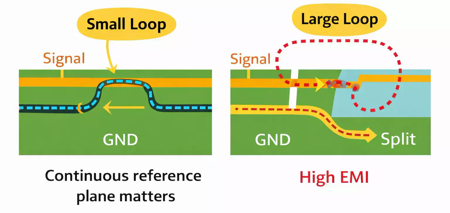
Reference adjacency. High-speed and controlled-impedance traces need a solid ground or power plane on the next dielectric layer. Distance to that plane sets the ohms target with width and copper weight. If the nearest copper is a fragmented pour two layers away, the return current invents a longer loop and EMI rises.
Continuous return path. Fast edges follow the lowest inductance path under the trace. Crossing a split plane, a slot, or a poorly stitched domain boundary forces that return around the gap. The detour radiates. Keep plane continuity under critical nets, and stitch domains deliberately when mixed-signal partitions require splits.
Symmetry and copper balance. Lamination shrinks resin and copper at different rates. An unbalanced stack -- thick copper on one side, thin cores on the other, or signal-heavy outer layers without mirrored construction -- bows and twists. Warpage that looks like an assembly fixture problem often started as an asymmetric stackup. Match CTE when mixing laminate families in a hybrid build; mismatched expansion shows up as registration shift and bow after press.
Avoid parking two signal layers against each other without a plane between them when crosstalk and EMI matter. Orthogonal routing helps when adjacency cannot be avoided, but a plane between signal layers is the cleaner default. Registration between layers after press is a manufacturing tolerance (often discussed near 50 um class for layer-to-layer); designs that assume perfect alignment on fine features will see annular-ring and impedance surprises.
Factory sequence that explains yield
Yield stories make more sense when you walk the panel the way the shop does.
Inner imaging and etch come first. Photoresist defines each inner copper layer; etch removes unwanted foil. Opens, shorts, and under/over-etch here become buried defects after press -- expensive to find and impossible to rework cleanly.
Layup and press follow. Cores and prepreg sheets are stacked to the agreed construction, then laminated under heat and pressure. Voids, resin starvation, and misregistration at this step become warpage, delamination risk, and thickness error. Hybrid materials with different CTE need press recipes the fab has already proven.
Mechanical drill (and laser drill for HDI) opens vias and component holes in the laminated stack or in sub-laminations. Drill quality sets annular ring and plating throw. Desmear cleans resin smear from hole walls so copper can adhere.
Electroless seed and electrolytic plate build conductive barrels. Thin mid-barrel plating is a reliability problem that electrical test on day one can miss and thermal cycling later reveals.
Outer imaging and etch pattern the top and bottom. Solder mask, silkscreen, and surface finish close the fab path, then electrical test checks continuity and isolation. Impedance coupons, when specified, verify that dielectric and etch landed inside tolerance -- commonly discussed around +/-10% unless a tighter callout is agreed.
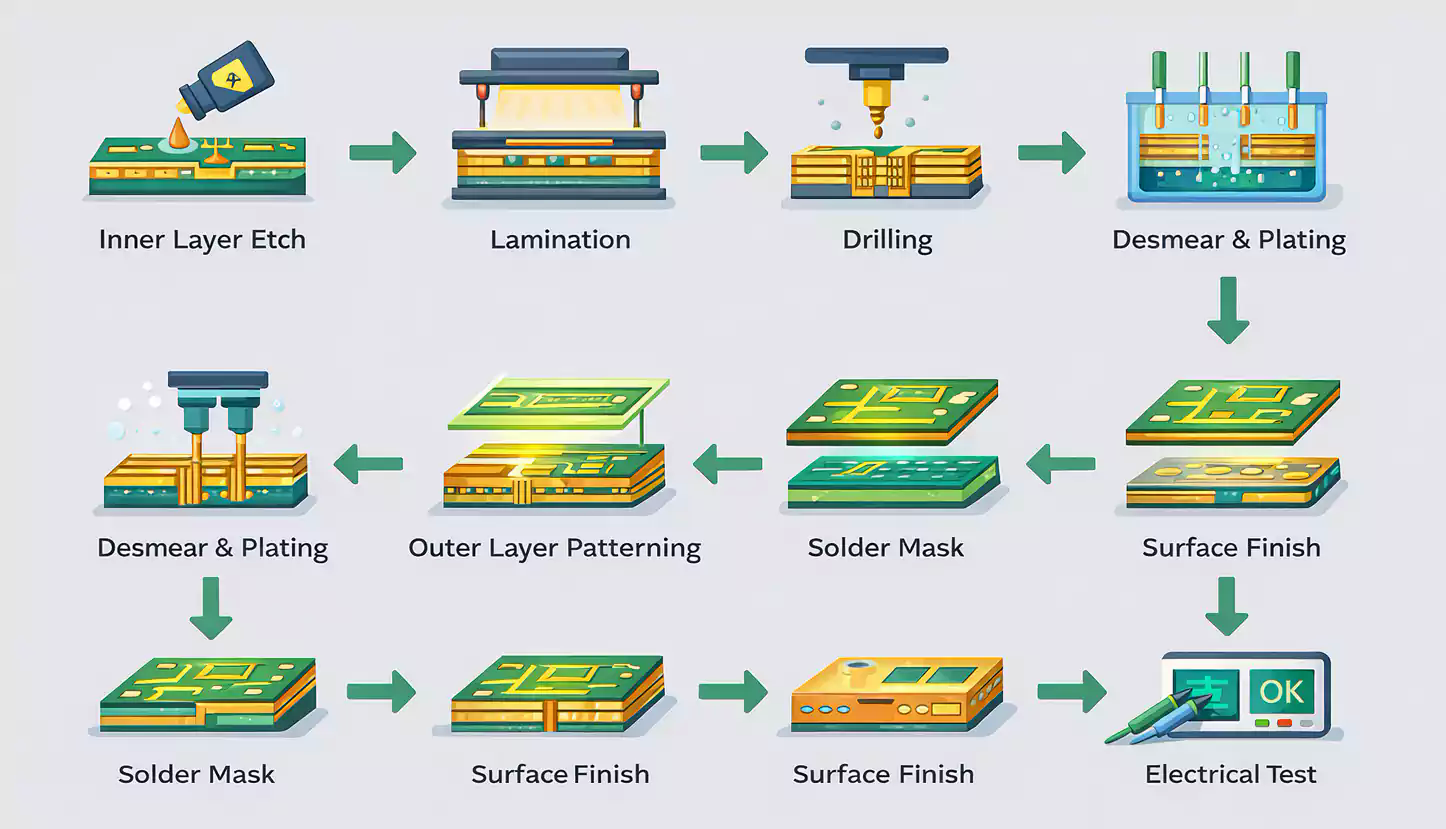
Each extra lamination cycle repeats thermal stress. That is why HDI and buried-via menus cost more than a single-press through-hole multilayer with the same outline: the panel is cooked and pressed more times before it ships.
What belongs on the stackup drawing for an XFPCB RFQ
CAM does not guess a construction from Gerber filenames. Put the contract on one drawing or note set that matches the files you want priced.
Include layer names and roles (signal, ground, power, mixed), core and prepreg material types, dielectric thickness per layer, copper weight per layer and finished copper after plating, total finished thickness with tolerance, and target impedance with reference layer, trace geometry, and tolerance. Call out via types and which layers they connect. If impedance is not required, waive it explicitly so quotes stay comparable. For hybrid builds, name both laminate families and ask for CTE-compatible press guidance. Attach the same revision of stackup notes to Gerbers or ODB++, NC drill, and fab notes.
For multilayer builds, point the RFQ at XFPCB multilayer capability and impedance control notes when controlled traces are in scope, and keep the manufacturing file package aligned to one revision. Early alignment on a stocked menu versus a custom press is usually cheaper than discovering mid-layout that the BGA forced another lamination cycle.
A board that survives schematic review still fails in the chamber or on the press when stackup is late. Lock layer count from density and rails, name via technology before routing burns the budget, write reference and symmetry rules into the drawing, and send XFPCB a stackup that matches the files -- that is the path that keeps CAM questions short and yield predictable.