
The first articles passed visual inspection. Pads looked wet, polarity matched the program, and the traveler closed green. On the bench the rails came up. Then Wi-Fi TX fired, or a motor stalled at peak current, and the MCU reset. Oscilloscope on the rail showed a dip and a burst of ringing that no AOI camera could have seen. The schematic was not "wrong." The power section was laid out like a signal board: pretty nets, long loops, and a stackup that looked correct on paper while the switcher return path was cut under the hot loop.
That is the procurement and technician problem this guide solves. A PMU (power management unit) on a PCB is the power section that regulates rails, sequences bring-up, and keeps loads alive under transient current. A PMIC is the chip at the center of that section. Buyers who treat the PMU as "just connect VIN and VOUT" get boards that assemble cleanly and fail under load, EMI, or heat. This article is for overseas PCB procurement managers and PCB technicians writing layout expectations and fab notes for China fabrication and assembly -- power-section layout and manufacturability, not a general high-power copper essay and not a multilayer stackup encyclopedia.
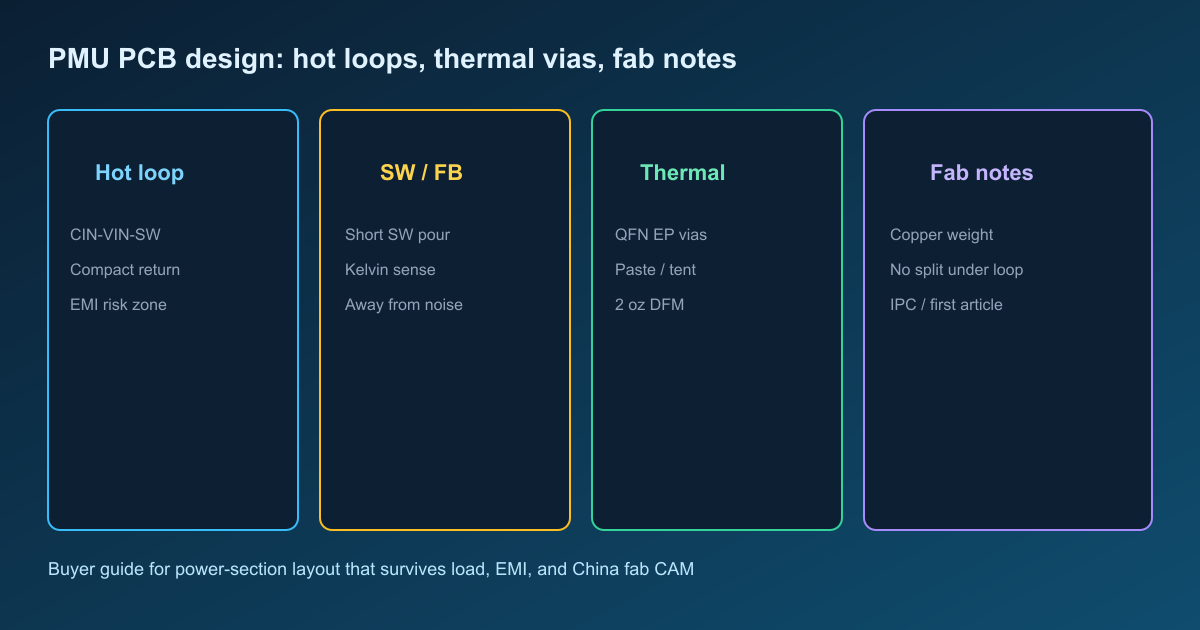
PMU versus PMIC in buyer language
PMIC means the power management integrated circuit -- the QFN, BGA, or module that switches, regulates, and often sequences multiple rails. PMU means the whole power block on the board: that IC, inductors, input and output ceramics, feedback networks, LDO stages, protection FETs, and the copper that carries current and heat.
Why the distinction matters on an RFQ: a quote that "builds the Gerbers as drawn" can still ruin a PMU if copper weight, via-in-pad, thermal via treatment, and contiguous ground under the switcher are left to CAM guesswork. The chip datasheet is necessary. The fab note pack that protects the layout intent is what makes quotes comparable.
Place the power stage before pretty signal routing
Layout order decides whether the hot loop stays small or becomes a late-route compromise.
- Place the PMIC / regulator island so VIN, SW, inductor, and load paths can stay short without crossing sensitive analog or RF keep-outs.
- Place the DC-DC power stage as one compact island: input ceramic, IC, inductor, output ceramic, then feedback resistors.
- Place LDOs near the loads that need quiet rails (ADC, RF, sensor, reference), with local ceramics at the pins.
- Route feedback, enable, power-good, and serial control last -- away from SW copper and inductor fields.
- Only then finish decorative signal packing and silk that does not change current paths.
Teams that route clocks and connectors first often discover the inductor has nowhere to sit except over a plane split. That is a field reset waiting for TX current, not a silk problem.
Hot loop, SW node, and feedback in practice
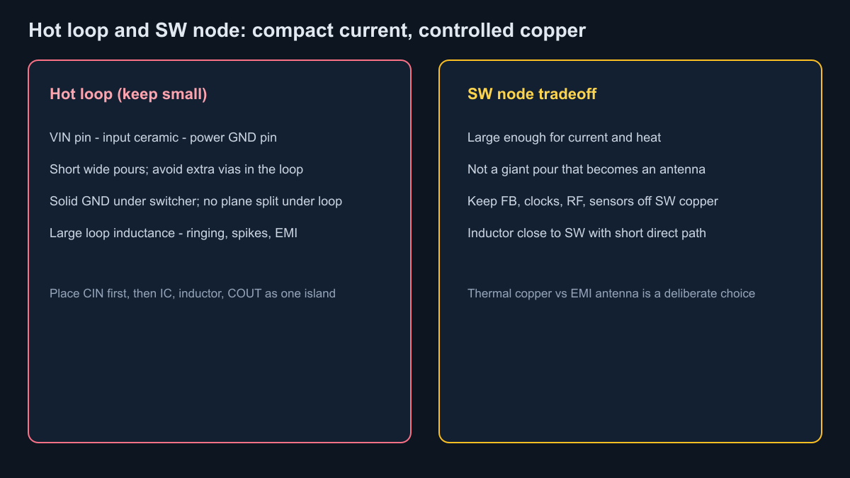
The hot loop is the high di/dt path: typically VIN pin to input ceramic to power ground pin (and the matching switch path into the inductor). Loop area sets parasitic inductance. Inductance becomes ringing, spikes, and radiated EMI. Keep pours short and wide. Avoid sprinkling vias through the loop "for neatness." Put a contiguous ground reference under the switcher; do not open a split under that island because a signal via needed a clearance elsewhere on the board.
The SW node needs enough copper to carry current and help heat leave the package. It does not need a decorative pour that acts like an antenna. Size it for current and thermal spreading, then stop. Keep feedback, clocks, reset, RF feeds, and sensor lines off SW copper and out from under the inductor.
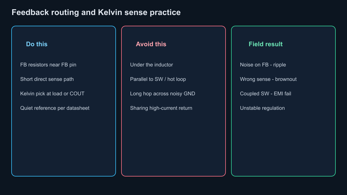
Feedback decides whether the regulator measures the rail you care about or the noise you created. Place divider resistors close to the FB pin. Use a short sense path; when the datasheet calls for Kelvin sensing, pick the sense point at the output capacitor or at the load per that note -- not halfway along a skinny trace that shares return with the switcher. Keep FB away from SW, away from the inductor, and off parallel runs next to high-current edges.
Ground is a return path, not leftover flood. Follow the vendor datasheet (or PMIC application note) for AGND / PGND joining: often a single star join or a specified pin region, not random stitch vias everywhere. Local HF ceramics belong at the pins with short ground vias into the plane. Plane inductance from a remote bulk cap does not replace pin-local ceramics.
LDO: noise versus heat, and when the package cooks
LDOs win when a rail must stay quiet for analog or RF. They lose when (VIN - VOUT) times load current dumps watts into a small package with no copper to leave. Place input and output ceramics at the pins. Give the package copper pour and thermal vias into a plane. If dropout heat is high, question whether a small switcher should feed a quieter post-LDO instead of asking an LDO to drop several volts at amps.
Overheat on an exposed-pad QFN is often assembly physics, not "bad silicon": starved center-pad paste, open vias stealing solder, or voids under the pad that block the heat path the layout assumed.
Stackup choice for return path: 2 versus 4 versus when more
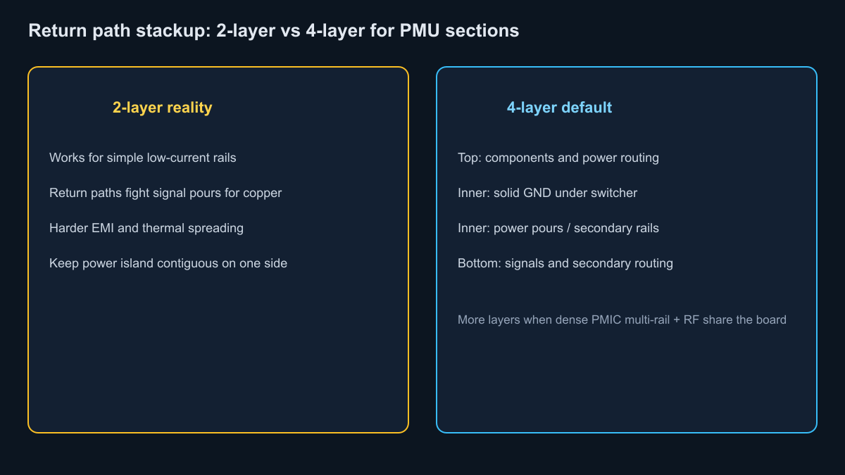
A 2-layer board can carry a simple low-current PMU if the power island stays contiguous and EMI limits are relaxed. Return current then fights every signal pour for copper. Dense multi-rail boards on 2 layers often fail EMI or brown out under load even when etch looks fine.
A 4-layer construction is the practical default for compact or noisy switchers: top for components and power routing, a solid inner ground under the switcher, an inner power or secondary pour layer, bottom for signals and secondary routes. Plan dielectric and copper weight early so impedance-controlled nets and heavy power copper do not surprise CAM.
More layers earn their keep when a dense PMIC, many sequenced rails, and RF or high-speed interfaces share one board and need separated references. Extra layers do not fix a large hot loop or a feedback trace under an inductor.
Power sequencing and multi-rail bring-up buyers rarely see in fab blogs
Many field "brownouts" are sequencing, not fab etch. Soft-start caps and enable timing set how rails ramp. If a downstream rail enables before its upstream input is solid, the PMIC can hiccup, UVLO, or reset the MCU while the oscilloscope still shows "some voltage" on average. Document rail order, soft-start targets, and power-good dependencies in the bring-up plan. On first article, check enable edges and rail rise times under the same load steps that will hit Wi-Fi TX or motor stall -- not only at idle.
When multi-rail boards fail only after assembly at one shop, ask whether enable pull-ups, soft-start values, and load timing match the design note before blaming copper. Layout still matters: a weak input path makes sequencing look broken when the real issue is voltage collapse at the VIN pin during the ramp.
Factory DFM: thermal vias, exposed pad, and heavy copper reality
Exposed-pad PMICs need a via array into ground or a thermal plane. Open vias under the pad can steal solder during reflow and leave voids that raise thermal resistance. Call out tented, plugged, or filled via-in-pad when the package and paste design require it. Stencil design for the center pad (window or window-pane) balances paste volume against float and void. First-article X-ray on the exposed pad is cheap insurance when the package is the thermal bottleneck.
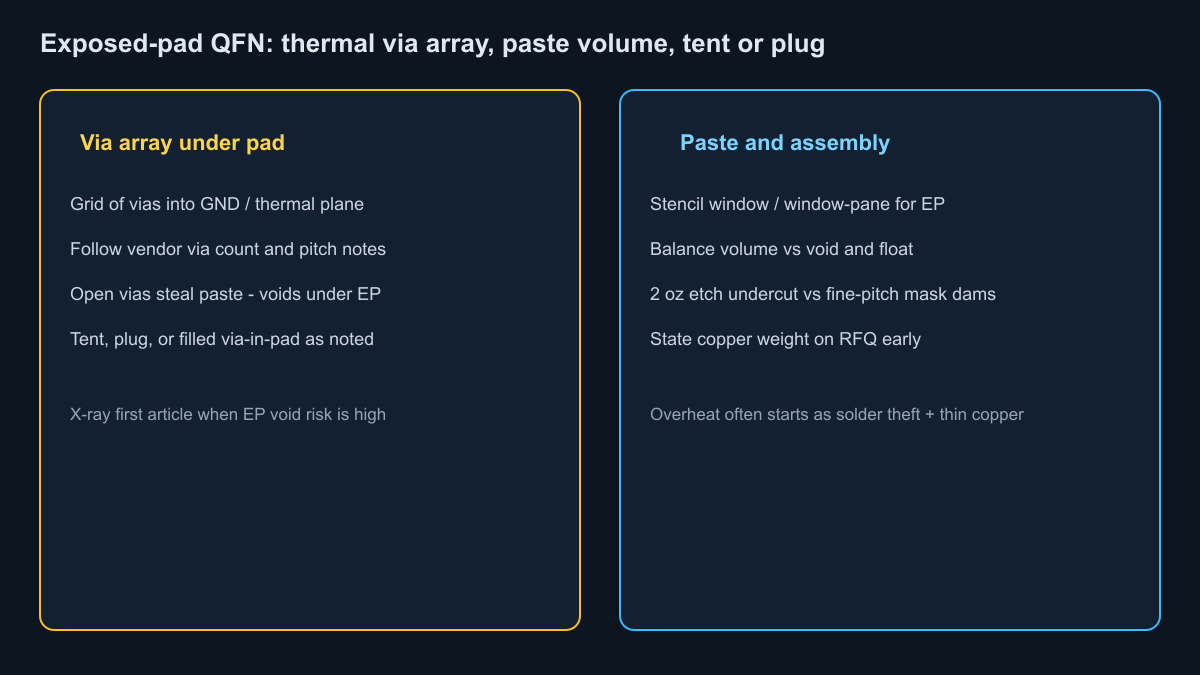
Heavy copper (for example 2 oz) cuts IR drop and spreads heat, but etch undercut grows, fine-pitch mask dams get harder, and solderability windows change. State finished copper weight per layer on the fab note. Do not assume a quote shop will "upgrade copper" silently without asking about clearance to a fine-pitch PMIC. Extra copper weight and via-in-pad fill also move cost and lead time -- put them on the RFQ so quotes stay comparable.
Field failure map: mistake to symptom
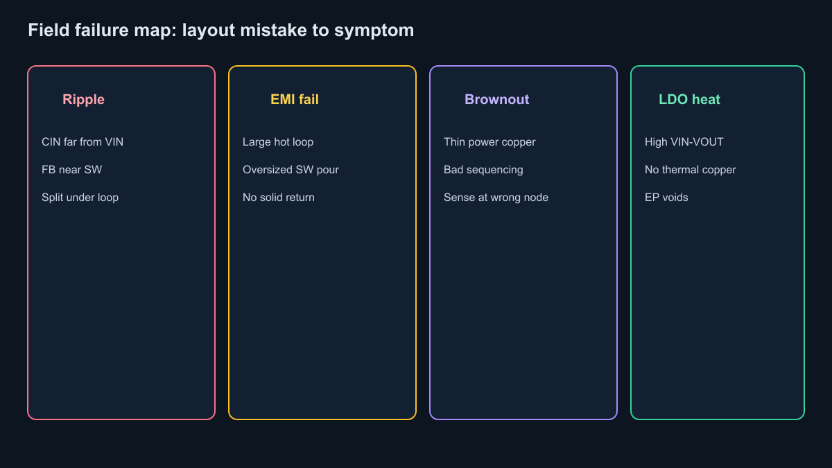
- Ripple and unstable regulation: input ceramic far from VIN / PGND, feedback near SW or under the inductor, plane split under the hot loop.
- EMI fail at certification or near a radio: large hot loop area, oversized SW pour, missing solid return under the switcher, noisy returns shared with analog.
- Brownout / reset under TX or motor load: undersized power copper or via count, sense point at the wrong node, sequencing that enables loads before the upstream rail is ready.
- LDO or PMIC overheat: high VIN-VOUT dissipation without copper, exposed-pad voids from solder theft through open vias, thermal vias missing or disconnected from plane.
Probe tips for first-article ripple without creating the noise
Ripple measurements lie when the probe ground lead is a loop antenna. Use a short ground spring or tip-and-barrel method at the output ceramic, not a long alligator ground across the board. Measure at the load and at the regulator output when diagnosing sense errors. Capture Wi-Fi TX or motor stall as a trigger event; idle ripple is not the failure mode that reset the MCU. If the scope shows hash that moves when you move the ground lead, you are measuring the probe, not the rail.
Fab notes and RFQ pack buyers should attach
Attach explicit notes so CAM does not "helpfully" split ground or thin copper:
- Finished copper weight per layer (call 2 oz where IR drop or heat demands it).
- Contiguous ground under the switcher; no plane split under the hot loop.
- Via-in-pad or thermal-via tent / plug / fill requirements under exposed pads.
- IPC class for fab and assembly acceptance.
- First-article expectations: rail ripple under stated load steps, thermal check on the PMIC case or board near the pad, and sequencing / soft-start confirmation on multi-rail boards.
- Stackup sketch with which layer is the solid reference under the power island.
- Any heavy-copper clearance or mask-dam constraints near fine-pitch PMIC pins.
A board house can etch a stackup that matches thickness and still ruin return paths if these notes are missing. That failure is not "bad fab luck"; it is missing intent on the drawing.
Closing
PMU PCB work is current-path, return-path, noise, heat, and bring-up discipline. Place the power island first. Keep the hot loop small, the SW pour honest, and the feedback quiet. Choose layer count for return path, not for brochure layer counts. Write thermal-via, copper-weight, and no-split notes into the fab pack, and prove rails under the same load steps that will hit the field. Visual AOI closes the traveler; load, EMI, and heat decide whether the PMU actually powers the product.