
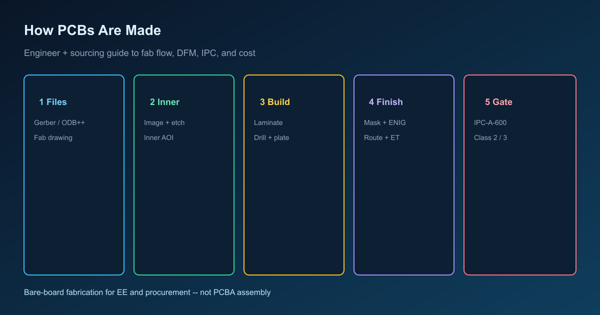
Bare-board fabrication turns Gerber or ODB++ copper patterns into a laminated, drilled, plated, masked, finished, and electrically tested PCB -- not an assembled PCBA. For engineers and buyers, "how PCBs are made" means the fab sequence that sets DFM risk, IPC-A-600 Class 2/3 acceptance, aspect ratio limits, surface-finish cost, and quote lead time before any SMT paste hits the panel.
This guide walks the multilayer fab flow from file package through CAM/DFM, inner etch and AOI, layup, drill/desmear/electroless, outer plate/etch, solder mask, ENIG/OSP/HASL finish, profile, and bare-board electrical test. It separates engineering tolerances from procurement cost and schedule levers so RFQs compare the same process, not marketing slogans.
What "how PCBs are made" really means for fabrication
Bare-board fab is the factory process that builds copper interconnects on FR-4 Tg or specialty laminates into a finished PCB that meets IPC-6012 Class 2 or Class 3 performance and IPC-A-600 visual criteria -- before components are placed. Assembly (paste, placement, reflow) is a separate cost center with different inspection language and different scrap economics.
Procurement teams that conflate fab with PCBA underpay for coupons, impedance control, or Class 3 plating while over-specifying assembly gates that never touch the bare board. Engineers who treat fab as a black box discover aspect-ratio, mask-dam, and copper-weight limits only after CAM engineering questions freeze the schedule.
The practical definition: files go in; a laminated, drilled, plated, masked, finished, profiled, and netlist-tested board comes out. Everything between those endpoints is where yield, cost, and Class depth are decided.
Files that start the job: Gerber, ODB++, fab drawing, and netlist
A manufacturable bare-board job starts with complete Gerber (or preferred ODB++ / IPC-2581), NC drill, a fabrication drawing with stackup and finish notes, and a netlist such as IPC-D-356 -- not a lone ZIP of copper layers without acceptance class. Missing notes force CAM to guess copper weight, solder-mask color, ENIG thickness, or Class 2 versus Class 3, which is how quote and traveler diverge.
ODB++ and IPC-2581 packages reduce layer-name ambiguity versus classic RS-274X Gerber sets, but they still need human fab notes for FR-4 Tg, oz copper, impedance targets, and surface finish. The fab drawing owns IPC-A-600 class, board outline, controlled-impedance coupons, and special processes such as backdrilling or microvia build-up.
Engineering & DFM Tip: Name every copper and mask layer consistently, include plated versus non-plated hole attributes, and call out minimum trace/space and annular ring on the drawing so DRC and CAM use the same numbers.
Cost & Lead Time Impact: Incomplete file packages trigger engineering queries (EQ) that pause the clock; a clean ODB++ plus IPC-D-356 netlist usually shortens CAM and reduces first-article surprises.
馃挕 Procurement Insight: Price apples-to-apples RFQs by attaching the same Gerber/ODB++ revision, fab drawing, stackup, finish, Class, and quantity breakpoints to every supplier -- not a verbal "standard FR-4 board."
CAM and the DFM gate
CAM engineering is the mandatory translation of your CAD output into panelized tooling, etch compensation, and drill programs, and the DFM gate is where manufacturability conflicts are raised before copper is etched. Skipping or delaying this step does not save time; it moves failures into scrap after inner etch or final electrical test.
Typical CAM checks cover minimum trace/space versus process capability, annular ring, aspect ratio, solder-mask dams/bridges, copper balance, and whether impedance stackups match available cores and prepregs. DFM warnings on acid traps, isolated copper, or insufficient mask clearance are cheaper to fix in layout than after lamination.
- Import files and normalize layer map (time sensitivity: EQ replies within hours keep quick-turn slots).
- Run DFM rule decks against Class and finish (yield sensitivity: early catch of annular ring and dam width).
- Panelize with coupons and tooling holes (yield sensitivity: copper balance and coupon placement).
- Release tooling only after customer sign-off on material EQ items.
Engineering & DFM Tip: Design to the fab's published Class 2 capability first; treat Class 3 and HDI microvia rules as deliberate upgrades with documented exceptions, not silent hope.
Cost & Lead Time Impact: Every open EQ can idle a panel queue; locked stackup and finish before CAM often saves a day on quick-turn and avoids requote after material substitution.
鈿狅笍 DFM Warning: "It passed DRC" only proves your CAD rules -- not the fab's etch, drill, and mask process windows that IPC-6012 and shop travelers actually enforce.
Inner layer image, etch, and inner AOI
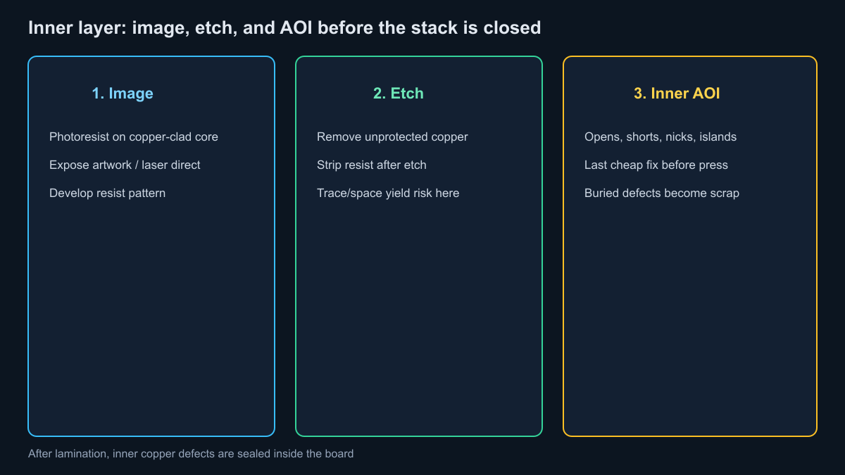
Inner-layer fabrication images photoresist on copper-clad cores, etches unwanted copper, strips resist, then runs automated optical inspection (AOI) because those copper features will be sealed inside the laminate after press. An open or nick that escapes inner AOI becomes buried scrap that flying probe may still catch late -- or miss if the net still "connects" through a hairline.
Fine etch on 0.5 oz or 1 oz copper sets the real minimum trace/space yield; claiming 3/3 mil without confirming process capability is a common RFQ mismatch. Copper balance across the core reduces warp risk later in lamination.
Engineering & DFM Tip: Keep isolated pads tied with teardrops or pours where signal integrity allows, avoid acute acid-trap angles, and match inner copper weight to the impedance stackup -- not an afterthought "default 1 oz."
Cost & Lead Time Impact: Tighter than capability etch and heavy copper raise scrap risk and may force slower etch chemistry or thicker starting foil; inner AOI adds minutes per panel but prevents high-value multilayer scrap after press.
Layup and lamination
Layup stacks etched cores, prepreg, and outer foil in the order defined by the stackup drawing, then lamination presses that sandwich under heat and pressure so resin flows and bonds into one rigid multilayer blank. Wrong prepreg count, swapped cores, or asymmetric copper is how warpage and impedance drift enter the traveler before any drill bit spins.
FR-4 Tg selection (for example Tg 135 versus high-Tg grades) and Rogers-class RF laminates change press cycles, moisture bake needs, and material lead time. Sequential lamination for HDI or buried vias multiplies thermal excursions and registration risk.
Engineering & DFM Tip: Freeze dielectric thicknesses and copper weights with the fab while schematic is still movable; odd-layer or highly asymmetric builds need explicit warp mitigation, not last-minute pours.
Cost & Lead Time Impact: Stock FR-4 constructions quote faster; hybrid Rogers-class or multiple sequential presses add material premium, longer bake/press queues, and higher scrap exposure.
Drill, aspect ratio, desmear, and electroless copper
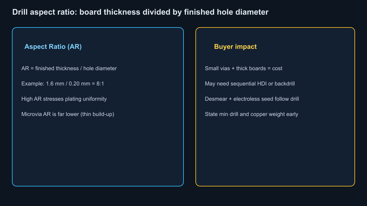
Mechanical drilling creates vias and component holes after lamination; aspect ratio (board thickness divided by finished hole diameter) plus desmear and electroless copper seeding determine whether plating will be reliable through the barrel. High aspect ratio and tiny drills drive broken bits, thin plating in the hole center, and reliability risk under thermal cycling -- especially for IPC-6012 Class 3.
Laser microvias on thin outer dielectrics use much lower aspect ratios and support HDI sequential build-up, but they add press cycles. Backdrilling removes unused plated stubs on thick high-speed boards after plating, trading an extra CNC step for cleaner signal integrity.
- Drill PTH and tooling holes (yield sensitivity: bit size vs thickness).
- Desmear resin smear from hole walls (yield sensitivity: smear left behind kills plating adhesion).
- Electroless copper seed, then electrolytic plate (time sensitivity: bath control windows).
- Optional backdrill of stubs after plate (cost sensitivity: extra CNC + inspection).
Engineering & DFM Tip: Cap aspect ratio within the fab's published PTH window; if density forces smaller holes, thin the board, split into HDI microvia build-up, or enlarge critical vias before CAM locks tooling.
Cost & Lead Time Impact: Small drills on thick boards raise bit cost and scrap; backdrilling and laser microvia steps each add process days and NRE-like programming time on new jobs.
Outer pattern: plate and etch
Outer-layer patterning defines pads and traces on the plated blank using either pattern-plate or panel-plate-and-etch flows so final copper geometry matches the Gerber while maintaining plated hole integrity and annular ring. Overclaiming outer etch density without matching inner capability or copper weight creates impedance and annular-ring surprises at coupon measurement.
Engineering & DFM Tip: Account for etch compensation and plating thickness when setting controlled-impedance line widths; 1 oz versus 2 oz copper changes both resistance and etch undercut behavior.
Cost & Lead Time Impact: Heavy copper and ultra-fine outer features both move the job out of commodity pricing and can extend plating or etch queue time.
Solder mask, dams, and bridges
Liquid photoimageable (LPI) solder mask is applied, imaged, and cured to open pads while leaving mask dams between fine-pitch pads and mask bridges over copper that must stay insulated -- a yield-sensitive step that later decides SMT bridge rates. Mask registration error, insufficient dam width, or poorly tented vias become assembly defects that look like "fab quality" disputes even when copper nets tested clean.
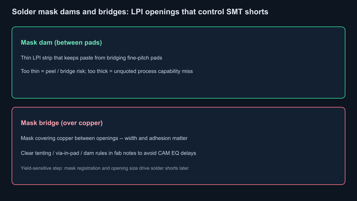
Engineering & DFM Tip: Respect the fab's minimum mask dam and bridge widths for your pitch; call out via tenting, plugging, or via-in-pad fill explicitly so CAM does not invent a default.
Cost & Lead Time Impact: Nonstandard colors, selective hard-gold fingers, or via-plug processes add steps; mask rescreens after EQ burn schedule on quick-turn panels.
鈿狅笍 DFM Warning: Designing 0.4 mm pitch pads with dams thinner than process capability forces either a CAM reject or a silent dam removal that raises bridge risk at SMT.
Surface finish: ENIG, OSP, HASL, and peers
Surface finish is the final solderable coating on exposed copper -- ENIG, OSP, HASL (usually lead-free), immersion silver, or immersion tin -- chosen for flatness, shelf life, wire-bond needs, and cost rather than habit. The finish does not replace good plating or mask; it only protects and prepares pads for assembly.
| Finish | Flatness | Shelf / handling | Typical use | Cost trend |
|---|---|---|---|---|
| ENIG | Excellent | Long, robust | Fine pitch, BGA, Al wire bond | Higher |
| OSP | Excellent | Shorter; reflow-limited | High-volume SMT, cost-sensitive | Lower |
| HASL (LF) | Fair to good | Robust | Through-hole, coarse pitch | Lower |
| Immersion Ag | Very good | Humidity sensitive | Fine pitch alternative | Mid |
| Immersion Sn | Good | Whisker / window limits | Press-fit / select SMT | Mid |
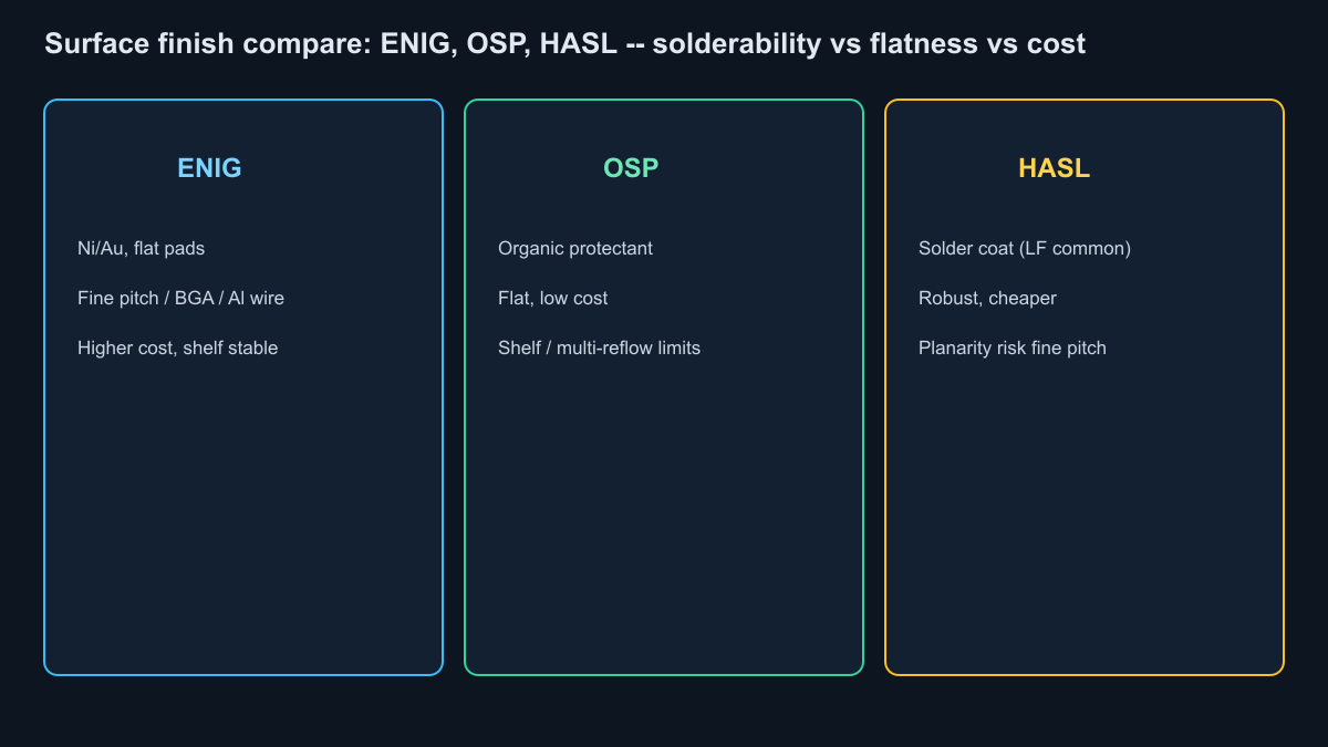
Engineering & DFM Tip: Match finish to pitch and assembly thermal budget -- ENIG for flat fine-pitch pads, OSP when controlled handling and short shelf windows are acceptable, HASL when planarity is not critical.
Cost & Lead Time Impact: ENIG adds chemistry time and gold cost; OSP is usually fastest and cheapest but can force tighter logistics; mixed finishes on one board raise process complexity and quote.
馃挕 Procurement Insight: Never compare quotes that silently swap ENIG for OSP; finish changes both unit price and field solderability risk under the same IPC-A-600 Class label.
Profile, route, and score
Board outline separation by CNC route, V-score, or punch defines the final PCB shape and panel breakaway method after finish, and poor outline definition is a common source of dimensional rejects under IPC-A-600. Edge plating, gold fingers, and tight outline tolerances need explicit fab notes because scoring and routing leave different edge quality and different panel utilization.
Engineering & DFM Tip: Provide a clear outline layer, keep copper and mask clearances from the route path, and specify mousebites or V-score depth when panelization matters for SMT.
Cost & Lead Time Impact: Complex contours, internal cutouts, and plated edges add CNC time; inefficient panelization raises unit price even when the board itself is simple.
Electrical test, IPC-A-600, coupons, and Class 3
Bare-board electrical test verifies opens and shorts against the netlist (flying probe or fixture), while IPC-A-600 sets visual/dimensional acceptance and IPC-6012 Class 2/3 sets performance depth -- including plating and reliability expectations that coupons help prove. Passing flying probe does not mean the board is Class 3, and IPC-A-600 Class 2 cosmetics do not prove impedance coupons met target.
| Topic | IPC Class 2 (typical) | IPC Class 3 (typical) |
|---|---|---|
| End use | Dedicated service, general electronics | High reliability / harsh duty |
| Annular ring / plating | Standard production windows | Tighter allowances, less defect tolerance |
| Inspection depth | Standard AOI + ET | Stricter criteria, more sampling/coupons |
| RFQ impact | Lower cost, wider fab pool | Higher cost, fewer capable lines |
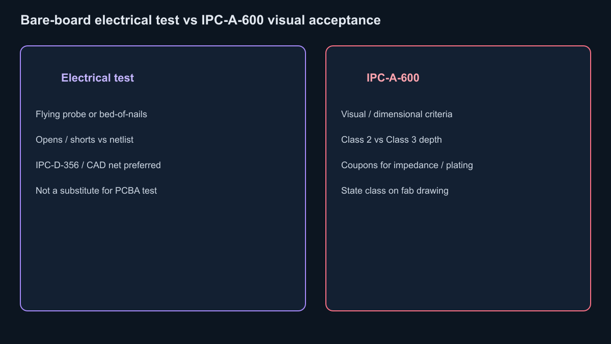
Engineering & DFM Tip: Supply IPC-D-356 or CAD netlist for ET; place impedance and plating coupons on the panel when controlled impedance or Class 3 plating thickness must be evidenced, not assumed.
Cost & Lead Time Impact: Flying probe suits NPI; fixture ET amortizes at volume; Class 3 and coupon reporting raise price and can add measurement queue time.
馃挕 Procurement Insight: Separate bare-board ET language from PCBA ICT/FCT in the RFQ so you are not paying twice for unrelated coverage -- or accidentally skipping one.
Advanced options: impedance, backdrilling, and HDI cost
Controlled impedance, backdrilling, and HDI sequential lamination with microvias are optional fab upgrades that buy signal integrity and density at the price of material control, extra CNC or laser steps, and more press cycles. They are not automatic with "multilayer" in the quote line.
Impedance control needs stackup lock, line-width compensation, and coupon measurement against target (often +/-10% unless tighter is stated). Backdrilling shortens stubs on thick boards carrying multi-Gb/s links. Blind/buried and laser microvia HDI reduce escape area but stack sequential lamination cost quickly when build-up layers multiply.
Engineering & DFM Tip: Specify impedance nets, reference planes, and tolerance on the fab drawing; call backdrill depth by layer pair; limit HDI to the minimum sequential cycles that actually solve BGA escape.
Cost & Lead Time Impact: Each added HDI build-up or backdrill pass is a schedule and yield lever; hybrid Rogers-class RF materials amplify both material lead time and process discipline needs.
Cost drivers master table
Total bare-board unit price is dominated by layer count, laminate family, copper weight, hole density and aspect ratio, surface finish, IPC Class depth, panel utilization, and special processes such as backdrill or HDI -- not by silkscreen color or logo cosmetics. Use the table below to steer RFQ trades before layout freezes the expensive options.
| Cost driver | Moves price up when... | Lead-time effect |
|---|---|---|
| Layer count / sequential presses | More layers or HDI build-ups | Longer press/drill queues |
| Material (FR-4 Tg, Rogers-class) | High-Tg, mid/low-loss, specialty | Possible material wait |
| Copper weight | 2 oz+ inner/outer | Slower etch/plate windows |
| Min hole / aspect ratio | Tiny vias in thick boards | Bit risk, plating risk |
| Surface finish | ENIG vs OSP/HASL | Chemistry time |
| IPC Class | Class 3 vs Class 2 | Tighter yield gates |
| Specials | Backdrill, impedance, via fill | Extra CNC / coupons |
| Panel utilization | Odd outline, low density | Higher unit cost |
How to evaluate a fab for Class 2 versus Class 3
A fab fit for IPC-6012 Class 2 may still be the wrong partner for Class 3 if plating thickness control, coupon discipline, cleanliness, and process capability evidence are weak -- Class is an acceptance and reliability depth, not a logo on the website. Ask for published aspect-ratio and min-feature capability, sample coupon reports, and how ET and IPC-A-600 criteria are applied on travelers.
RFQ checklist buyers can paste:
- Gerber or ODB++/IPC-2581 + NC drill + fab drawing + IPC-D-356 netlist
- Stackup with FR-4 Tg or Rogers-class callouts and oz copper
- Surface finish and solder-mask requirements
- IPC-A-600 / IPC-6012 Class 2 or Class 3 stated explicitly
- Impedance targets and coupon expectation if required
- Backdrill, microvia, via-fill, or gold-finger notes if any
- Quantity, panel preference, and lead-time tier
Related XFPCB guides
These related XFPCB guides extend this bare-board fab flow into DFM checklists, multilayer stackup decisions, inspection RFQ language, and quick-turn schedule tradeoffs without repeating the entire full fabrication process sequence.
Engineering depth
Engineering-depth guides dig into DFM rule themes and multilayer stackup construction that this fabrication-flow article assumes you will lock with the fab before CAM engineering releases tooling and final panelization.
- PCB DFM: Design for Manufacturing -- Use this when CAM EQ themes (annular ring, dams, trace/space) need a deeper design-side checklist before the next revision.
- Multilayer PCB Stackup Fabrication Guide -- Use this to lock layer order, dielectric thickness, and via architecture that this fab-flow article assumes are already decided.
Procurement decisions
Procurement-decision guides help buyers write comparable RFQ quality clauses and choose realistic lead-time schedule tiers after the bare-board fab process, Class depth, and cost drivers in this article are understood.
- PCB Inspection Methods Guide -- Use this to separate bare-board gates from PCBA SPI/AOI/X-ray/FCT language when writing RFQ quality clauses.
- What Is a Quick-Turn PCB? -- Use this when schedule tiers and which process options kill quick-turn feasibility matter more than unit price alone.