
The first article boots. LEDs blink. Then DDR traffic or a PCIe link-up spike hits, the core rail dips for a few tens of millivolts, and the SoC resets. AOI was clean. The Gerbers etched. The EMI lab later blames "layout." Procurement hears three different stories: not enough copper, wrong capacitors, HDI that was never filled. The common thread is usually the Power Distribution Network -- the loop that delivers current and takes it back -- not a single fat power trace that looked wide on a screenshot.
This guide is for overseas PCB procurement managers and PCB technicians buying and reviewing HDI boards from a China fab. It is about PDN and power integrity under dense BGA and microvia constraints. It is not a regulator hot-loop essay and not a general multilayer stackup encyclopedia. Those belong elsewhere. Here the job is stable rails when current steps, planes that still behave as capacitors after CAM, and via-in-pad that actually ships filled and capped.
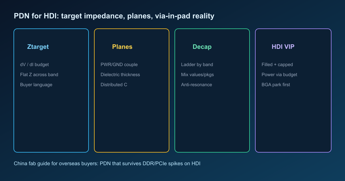
PDN is a loop, not a wide pour with a hopeful silk note
A Power Distribution Network is the path from the source (connector, battery, regulator output) through copper, vias, and capacitors to the IC power pins -- and the ground return that closes the loop. Current always travels in a loop. If the return is forced around a split, a clearance island, or a thin neck under a BGA, loop inductance rises. Inductance becomes voltage droop under fast di/dt, ground bounce, and radiated noise that shows up as an EMI fail long after the traveler closed.
On HDI boards the same physics is tighter: fine-pitch BGA, multiple core rails, DDR and SerDes neighbors, microvias that shorten some paths and starve others of park space. Quoting "HDI" without locking plane coupling, VIP fill, and power-via budget is how buyers pay for density and still brown out on first traffic.
Target impedance in buyer language (one worked example)
Vendor PDN methodology often states a target impedance for a rail:
Ztarget = allowed voltage ripple / transient current step
Worked example: a 1.0 V core rail allows 3% ripple, so allowed dV is 30 mV. A DDR or PCIe burst steps 2 A. Ztarget is 30 mV / 2 A = 15 milliohms. If the PDN impedance peaks above that number in the frequency band of the transient, the rail is allowed to leave the SoC budget -- resets become a matter of when, not if.
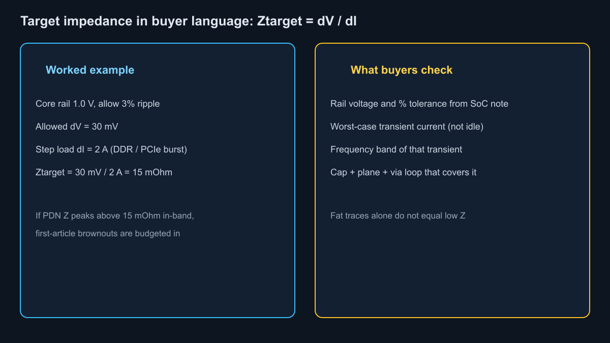
What to put on an RFQ conversation (not a tool UI dump): rail voltage, tolerance or absolute ripple limit from the IC note, worst-case dI (not idle), and the frequency content of that step. Bulk caps cover lower bands; mid and HF ceramics plus plane capacitance cover the rest. Fat traces without plane and via discipline will not hold 15 mOhm across a useful band.
Capacitor ladder by frequency -- and the same-value trap
Think in bands, not in a single BOM capacitor line:
- Bulk (often electrolytic or large ceramic near the regulator or board input): low-frequency energy storage and slow load changes.
- Mid-band decoupling: clusters near the BGA or load park, short vias into the power/ground planes.
- HF / bypass: small packages within a short electrical distance of the pin or ball (order of a couple of millimeters for the highest frequencies). Loop inductance dominates; value alone does not.
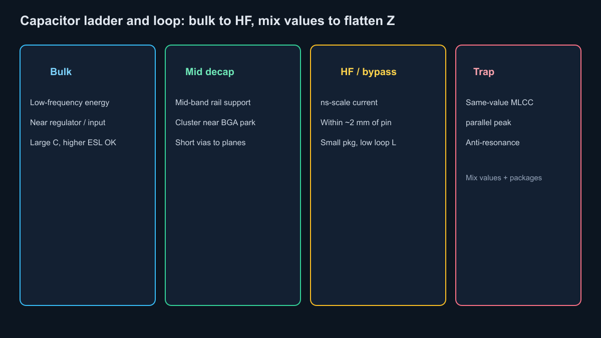
A common procurement trap is buying "ten of the same MLCC" because the schematic shows one value. Parallel same-value, same-package ceramics share a resonance; their interaction can create an anti-resonance peak where impedance spikes exactly where you needed it flat. Mix values and packages so resonances stagger and the composite Z stays closer to Ztarget. Placement still wins: a perfect mix far from the ball with long skinny necks behaves like a remote reservoir, not a local source.
Coupling capacitors on AC signal paths are not the PDN ladder; do not count them as rail support when reviewing the BOM against power integrity.
Planes as capacitors: dielectric thickness is a PDN part
Adjacent power and ground planes form a distributed capacitor. Plane capacitance scales roughly with area over dielectric thickness (C ~ eps * A / d). Thin dielectric between a contiguous PWR pour and a contiguous GND pour raises that capacitance and lowers spreading inductance -- exactly what HF current wants under a BGA.
When a signal layer is inserted into that sandwich "to gain a route layer," d grows and plane C collapses even if finished board thickness still matches the drawing title block. Buyers who quote HDI for microvias but accept a stackup that splits every power/ground pair lose the planar capacitor they thought they bought. Copper balance and warpage symmetry still matter for fab yield; PDN needs the pair spacing called out, not only total thickness.
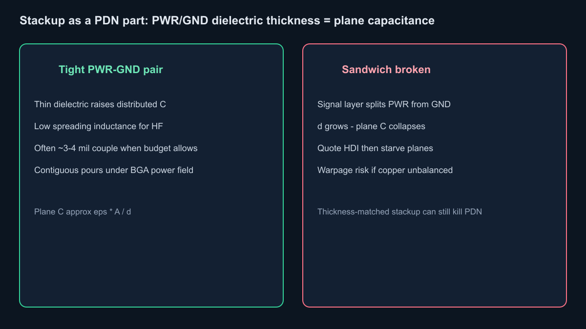
Practical notes from fab RFQs: call copper weight on power planes, require contiguous copper under the BGA power field (no clearance Swiss cheese for random stitching), and ask what dielectric thickness sits between the primary PWR/GND pair under that field. Impedance-controlled signal layers and PDN plane spacing are related stackup asks -- resolve them together so CAM does not thicken one couple to "help" impedance while starving PDN.
HDI structures that help or hurt PDN
Microvias, blind/buried vias, and via-in-pad can shorten the path from a power ball to an inner plane or to a bottom-side capacitor. That lowers loop inductance when the via lands on real plane copper and when fill/cap keeps the pad flat for solder.
They hurt when:
- Signal escape consumes every park site before power and ground vias are reserved.
- Unfilled VIP steals paste or leaves voids under BGA balls.
- Stacked microvia trees look dense on a 3D viewer but land on fragmented plane scraps.
- The build is deeper HDI than needed for signals while power still rides skinny necks on outer layers.
1+N+1 is often enough when outer microvias reach the first power/ground pair and the core carries contiguous planes. Deeper HDI earns money when power vias must reach buried planes under ultra-fine pitch without stealing the entire escape budget -- not because the brochure said "any-layer." Staggered versus stacked microvia is a reliability and cost choice; stacked builds need process control and clear fab notes. Equal-ish counts of power and ground vias near the core field keep the loop short; a forest of signal vias with two lonely power vias is a brownout pattern with pretty fanout.
Via-in-pad manufacturability buyers must lock
Via-in-pad for BGA power/ground balls usually means resin-filled and copper-capped (or an equivalent planarized VIP process the fab will own in writing). That gives a flat solderable pad, short ball-to-plane path, and a chance to put HF caps on the opposite side without a crater under the ball.
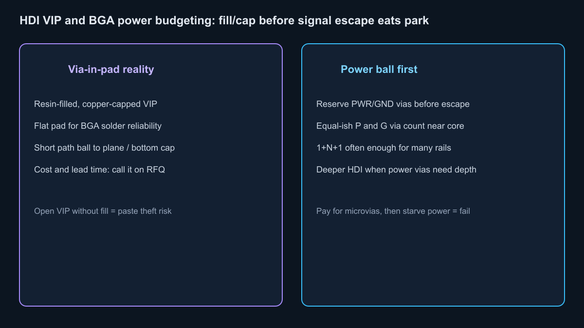
Open or poorly filled VIP is an assembly reliability risk and a PDN risk: paste loss, voids, and intermittent thermal/electrical contact. Put fill and cap on the RFQ. Price and lead time will move; that is honest HDI cost, not a surprise after Gerber release. Bottom-side caps under the BGA help only if the via path is short, filled correctly, and the park still has ground and power vias -- not signal-only escape with a lonely cap via.
Simulation when it earns money
PDN simulation (impedance versus frequency, transient droop, sometimes DC IR drop) earns its keep on multi-rail SoC/FPGA boards, dense HDI, and first articles that already failed once. It is not a substitute for plane coupling, via budget, and capacitor placement. A flat schematic C total with high mounting inductance still fails Ztarget.
Ask for simulation when: Ztarget is single-digit to low tens of milliohms, package pin inductance is known to be tight, or a previous spin reset under traffic. Skip it as theater when the stackup still splits PWR/GND under the BGA and VIP fill is "TBD." Fix the fab-intent gaps first; then simulate the layout you will actually build.
Failure map: symptom to PDN mistake
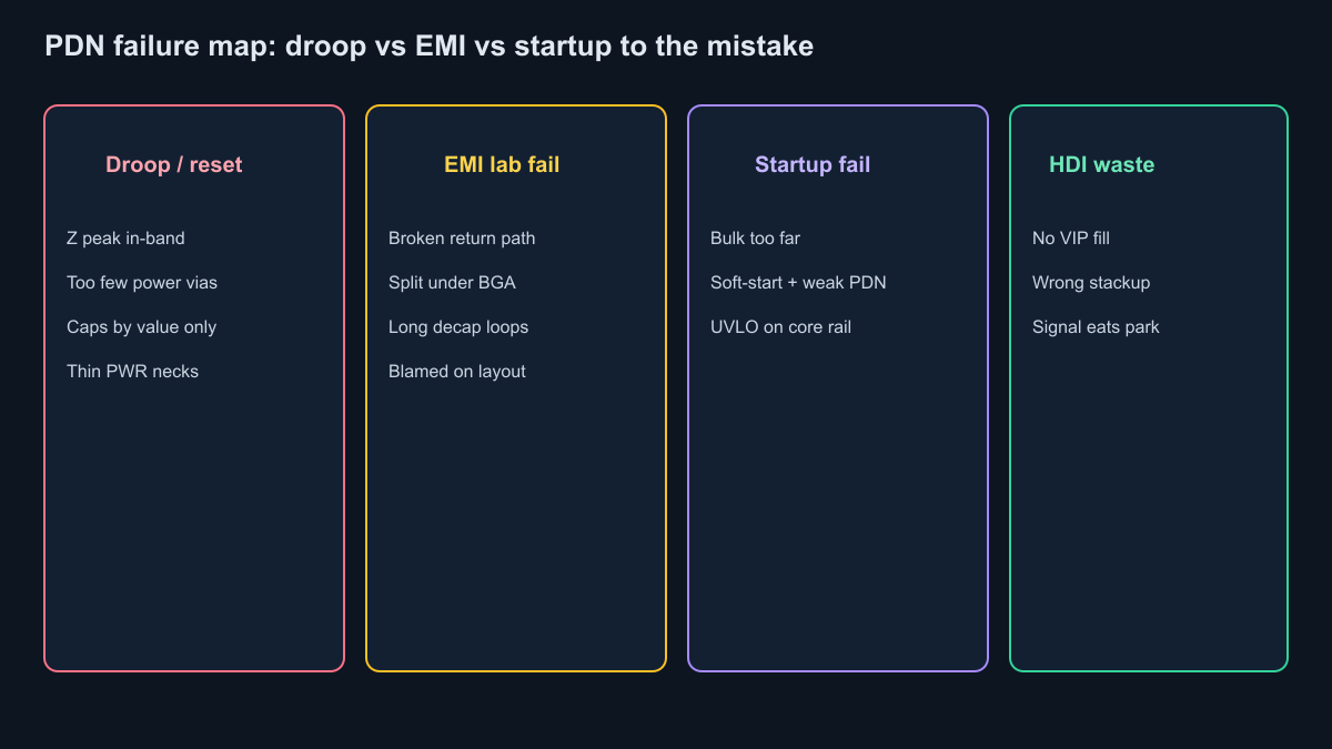
- Droop / reset under DDR or PCIe traffic: in-band Z peak (same-value anti-resonance or missing HF caps), too few power/ground vias under the BGA, thin power necks, caps chosen by value only and placed far from the ball.
- EMI lab fail blamed on layout: broken return path, plane split under the BGA or high-speed field, long decap loops that radiate, signal vias punching Swiss cheese through the reference.
- Startup / UVLO fail: bulk too far from the regulator or load during ramp, soft-start into a weak PDN, core rail collapsing while average voltage still "looks OK" on a slow meter.
- Paid for HDI and still failed: microvias without VIP fill/cap, stackup that destroyed PWR/GND couple, signal escape that ate the power via park.
Fab notes and RFQ pack for PDN on HDI
Attach intent so quotes are comparable and CAM does not "optimize" the PDN away:
- Finished copper weight per power and ground layer.
- Contiguous planes under the BGA power field; no unapproved clearance islands.
- Dielectric thickness / couple between primary PWR and GND under that field (PDN plane spacing), alongside any controlled-impedance notes.
- Microvia type (laser, stacked vs staggered) and build (for example 1+N+1 versus deeper).
- Via-in-pad: resin fill and copper cap (or named equivalent) for power/ground VIP.
- Power and ground via budget near core rails before signal-only escape is accepted.
- First-article ripple measurement expectation under defined traffic or load steps (probe method that does not invent noise with a long ground lead).
- IPC class and any X-ray expectation on VIP / BGA joints when fill quality is critical.
A thickness-matched coupon can still ship a dead PDN if these notes are missing. That is missing drawing intent, not random fab luck.
Closing
HDI PDN work is loop control: Ztarget from real dV and dI, a capacitor ladder that mixes values and packages, planes that stay close enough to act as capacitors, and vias that are reserved for power and ground before escape art wins. Lock VIP fill and stackup couple on the RFQ. Prove rails under the same traffic that will hit the field. Clean AOI closes the traveler; flat impedance under load decides whether the SoC stays up.
Related XFPCB guides
Continue with these XFPCB pieces when you are wiring power integrity to layout, stackup, and assembly reality: