
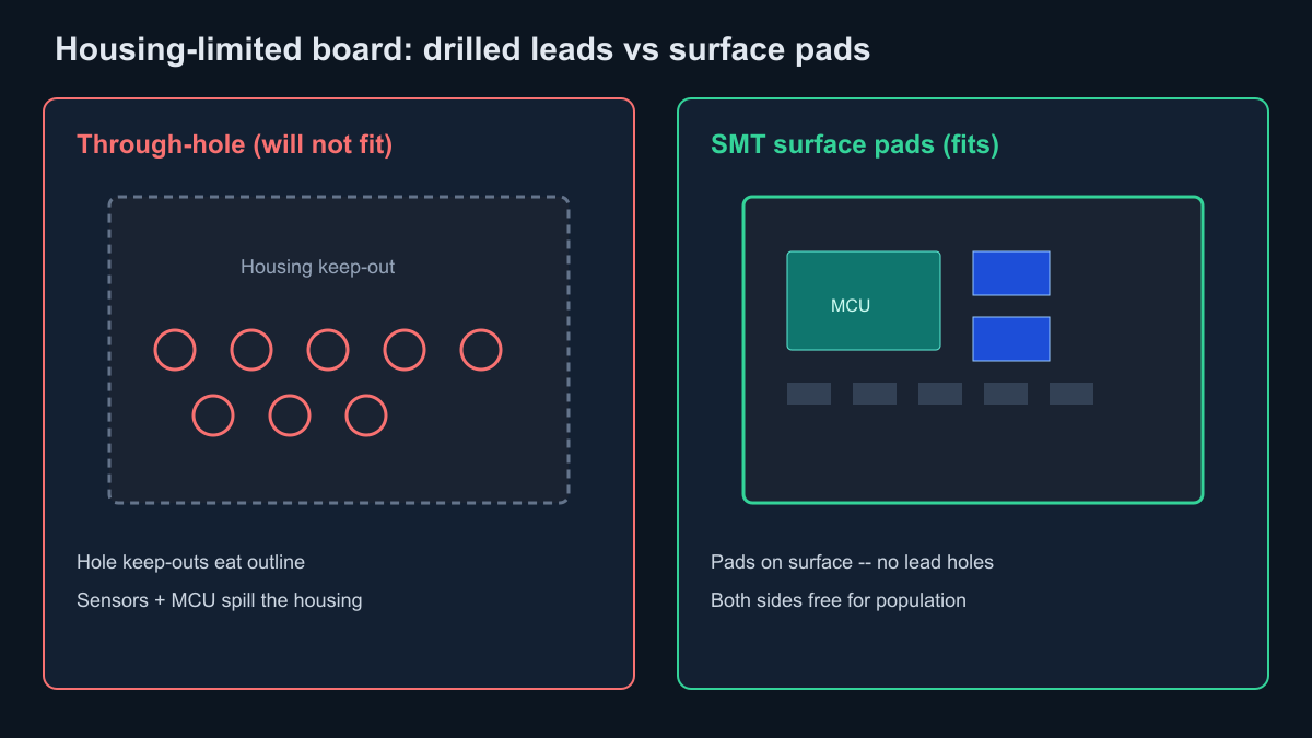
The mechanical envelope was locked: sensors on three faces, an MCU, radio, and a handful of passives inside a housing that had already been tooled. The through-hole layout still needed drilled leads for every package. Board area climbed, keep-outs around every hole ate routing, and the stack would not close without growing the plastic. That is the conversation product and layout teams have with mechanical and procurement when density is not optional -- and when surface mount is the reason the product fits, not a brochure preference.
This article is a China PCBA view of what SMT actually changes on the board for high-density designs: pads instead of drilled leads, both-side populate, shorter electrical paths for speed and RF, factory stencil and reflow discipline that density demands, where heavy connectors still belong in through-hole, applications that force the density call, and RFQ notes that keep fine-pitch and HDI assembly quotable. It is not a partner-selection checklist; it is the density case itself.
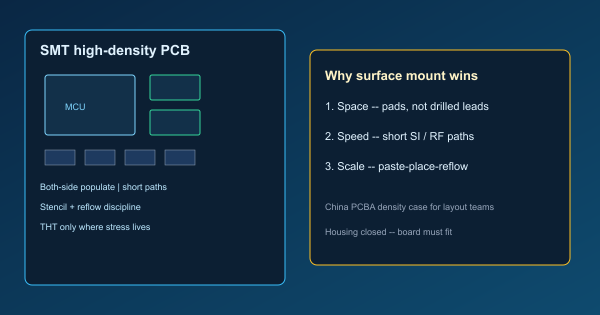
What SMT changes on the board: pads, not drilled leads
Through-hole assembly inserts component leads through plated holes and solders them on the opposite side (or both sides in some flows). Every lead consumes a drilled hole, annular ring, and keep-out that punches through the full stack-up. That hole steals routing on every layer it crosses and forces larger land patterns than the package electronics alone would need.
Surface mount places the part on copper pads with solder paste, then reflow. No lead hole per pin for the passives and ICs that dominate a modern BOM. Footprints shrink toward 0402, 0201, and finer when process and stencil allow. The same outline can hold sensors, an MCU, RF front-end, and decoupling that a PTH-first layout would push off the board or into a second PCB.
Both-side population is the second density lever. SMT parts sit on surface pads, so top and bottom can both carry active and passive loads when reflow sequence and thermal mass are planned. Through-hole leads that cross the board block that freedom and leave less internal copper for planes and escape. Multilayer routing benefits when via real estate is reserved for signals and power instead of component lead clearance.
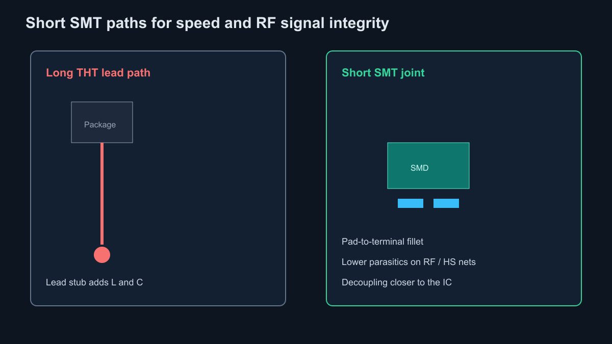
Short electrical paths for speed and RF
High-density boards often carry high-speed digital and RF nets in the same outline. Lead length is parasitic inductance and capacitance. SMT joints are short: pad to package terminal with a controlled solder fillet. That reduces loop area for return currents, helps impedance control when reference planes are close, and keeps decoupling capacitors within the loop the IC actually needs.
RF and high-speed layout still needs stackup discipline, controlled-impedance traces, and clean return paths. SMT does not replace those rules. It removes the long lead stubs that make those rules harder to meet on a through-hole-heavy board. Critical signal paths stay SMT; connectors and power interfaces may still use through-hole where mechanical retention wins -- hybrid is normal, not a compromise of principle.
Thermal paths also change with density. Low-profile SMT packages sit close to copper pads and planes that spread heat. Exposed thermal pads on power devices, thermal vias under QFN and BGA, and copper pours matter more as parts pack tighter. Heat is a layout and copper problem first; mounting style alone does not cool a crowded board.
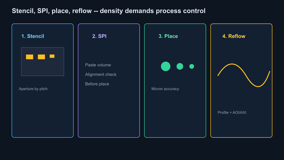
Factory throughput and stencil / reflow discipline density demands
Density that looks free in CAD is paid for on the line. SMT wins scale because pick-and-place and reflow are automated: paste print, place, reflow, inspect. Fine pitch and high part counts raise the bar on stencil aperture design, paste volume control, placement accuracy, and reflow profile matched to the thermal mass of the board and the packages on it.
What China PCBA lines enforce when density is real:
- Stencil thickness and aperture geometry matched to the finest pitch on the panel, not a one-size paste window.
- SPI (solder paste inspection) before place when fine pitch or bottom-terminated packages are in the mix.
- Reflow profiles that respect both large thermal pads and small passives on the same side.
- AOI after reflow, and AXI for BGA, QFN, and other hidden joints when the package mix requires it.
- Panelization and support that keep thin or dense boards flat through reflow.
Skipping drill for SMT leads removes a fab step and a placement bottleneck, but it does not remove process control. Tombstoning, bridging, insufficient solder, and voiding under thermal pads are density-adjacent defects. The throughput argument only holds when stencil, placement, reflow, and inspection travel with the design.
Where heavy connectors still need through-hole
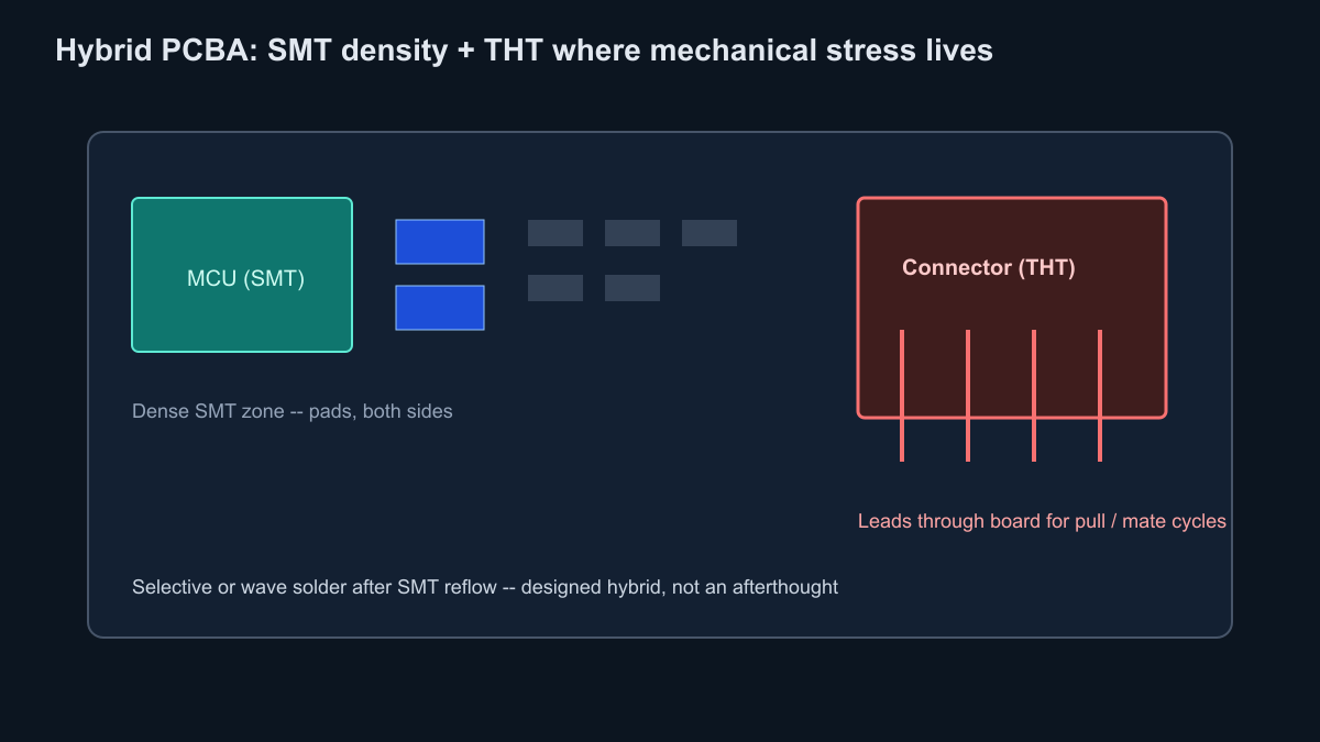
SMT is not a ban on through-hole. Connectors that see repeated mate/unmate cycles, terminal blocks under pull force, large transformers, relays, and heavy modules often need the mechanical retention of leads through the board -- or a hybrid with SMT signal pins and mechanical anchors. Wave, selective, or hand solder after SMT reflow is the usual mixed-technology sequence.
Procurement sometimes hears "all SMT" as cheaper forever. Mixed boards add insertion and secondary solder steps. That cost is often still cheaper than field failures from connectors lifting pads. Design the hybrid on purpose: SMT for density and SI, through-hole where stress lives, clearances for selective solder access, and inspection access called out on the drawing.
Applications that force density
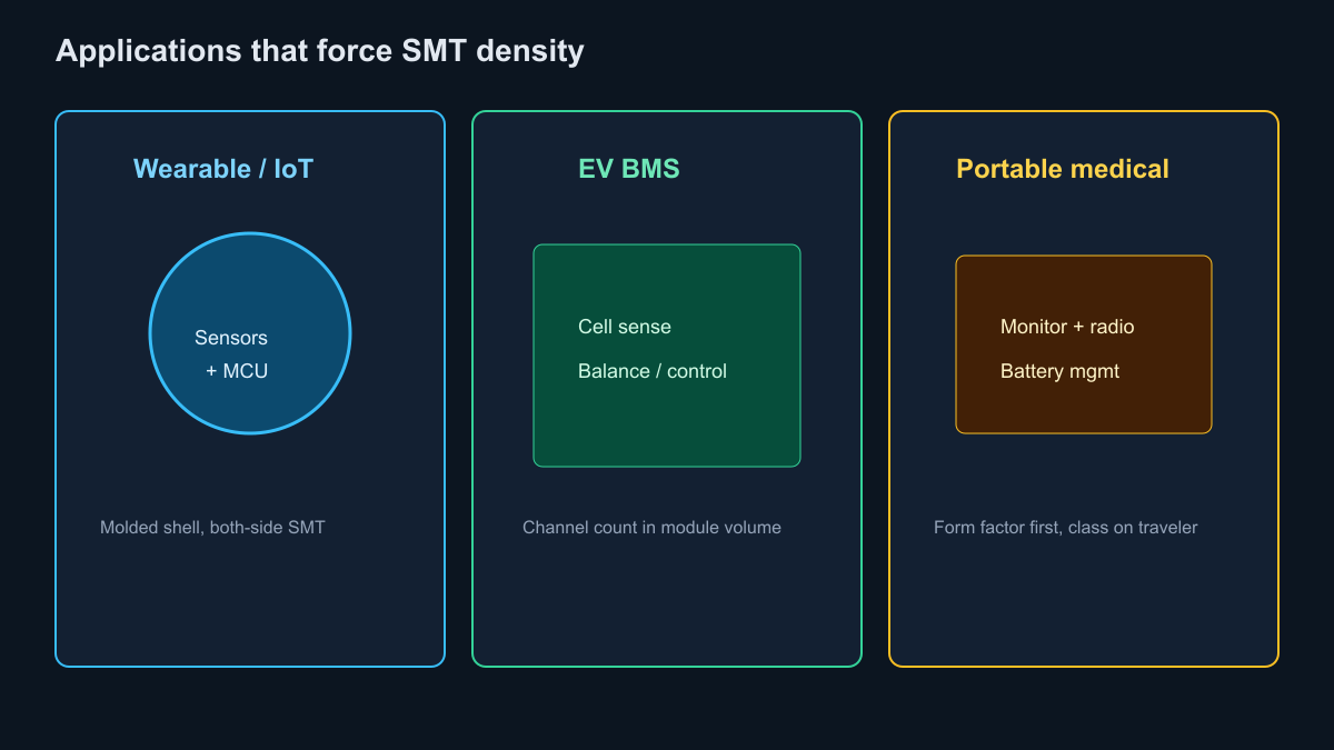
Wearables and compact IoT modules: outline and weight budgets leave no room for PTH keep-outs around every passive. Both-side SMT and fine pitch are how sensors, MCU, and radio share one board inside a molded shell.
EV battery management and mobility electronics: cell sensing, balancing, and control want many channels in a constrained module volume. Density here is channel count and isolation spacing, not only consumer miniaturization -- SMT packs the measurement and control tree while connectors and high-current interfaces may stay through-hole or press-fit.
Portable medical monitors and diagnostic modules: small enclosure, multiple sensors, wireless link, and battery management on one or two boards. SMT density supports the form factor; process class, cleanliness, and inspection coverage follow the market -- still density-first on the layout, compliance-first on the traveler.
Industrial and communications modules follow the same pattern when the product must fit a DIN rail pocket, a sealed radio enclosure, or a camera module that cannot grow. Housing and connector pitch set the board size; SMT is how function fits that size.
RFQ notes for fine-pitch and HDI assembly
China fabs and PCBA houses quote what is written. Density language that stays in email produces CAM questions and non-comparable bids.
Put on the RFQ and drawing package:
- Package mix and finest pitch (including BGA / QFN / LGA pitch and ball or pad count).
- Whether both sides are populated and the intended reflow sequence (single vs double reflow).
- Via strategy tied to escape: through-hole only vs laser microvia / HDI build (1+N+1, 2+N+2, or higher) when fine-pitch escape needs it.
- Minimum line/space, via-in-pad fill and cap if used, and surface finish matched to fine-pitch wetting (often ENIG for flat pads).
- Stencil and paste assumptions if the buyer specifies them; otherwise ask the assembler to propose aperture rules for the finest pitch.
- Inspection: AOI scope, AXI for hidden joints, flying probe or ICT if required, IPC class on the drawing.
- Mixed technology: which connectors or power parts are through-hole, and selective vs wave access notes.
- One revision-aligned set: Gerbers or ODB++, centroids, BOM with MPNs, assembly drawing, and fab notes.
XFPCB builds SMT density as a construction and process plan -- pad geometry, stencil and reflow discipline, HDI escape when pitch demands it, and through-hole only where mechanical load requires it -- so the housing that already closed in CAD can ship as a manufacturable PCBA.
SMT wins high-density PCB designs because surface pads and both-side populate fit more function in a locked outline, short joints help speed and RF nets, and automated paste-place-reflow scales when stencil and inspection keep pace. Through-hole still owns stressed connectors and heavy parts. Write density, pitch, via type, and inspection as RFQ line items so China PCBA quotes match the board you actually need to release.