
The pilot panel cleared continuity and isolation. Every net that mattered measured green on the fixture. Two weeks later AOI flagged a row of 0402 resistors standing on one end, thermal camera maps lit a regulator island hotter than the enclosure budget, and the EMC bench failed a clock harmonic that never showed up in the schematic review. Electrical pass and production ready are not the same sentence. The gap sits in package choices that fight reflow, laminate properties that warp under thermal cycling, EMI zoning that left return currents hunting across domains, and copper that never had a chance to move heat before someone ordered a heatsink.
Layout engineers whose first assembly spin fails on tombstone, crosstalk, or hotspots land here. So do buyers who discover that package and material decisions made after RFQ become rework line items. This Part-2 style guide stays on components, materials, EMI zoning, and heat paths -- the decisions that prevent respins after the netlist already looked correct. It is not a DRC-to-CAM story and not a layer-count stackup tutorial; those live elsewhere. The goal is freezing the yield-critical choices before the quote so the first buildable panel is not an expensive experiment.
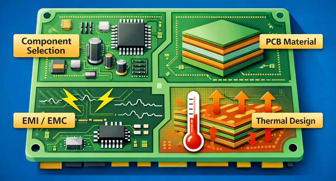
Package selection is a yield decision, not a catalog flex
Footprint size and pin pitch are electrical and mechanical choices, but they are also assembly-yield choices. Picking the smallest package that fits the outline often raises placement difficulty, paste-release risk, and inspection opacity without buying measurable electrical headroom. Mainstream packages with mature library footprints are easier to source, place, and verify across revisions. A disciplined library -- mechanical outlines, pad geometry matched to the datasheet, and supplier notes -- cuts the footprint mistakes that only appear after stencil and AOI.
Leaded fine-pitch parts deserve extra scrutiny. Industry practice often treats QFP pitches below about 0.5 mm as a caution zone for solder bridging, coplanarity, and rework access. When I/O density forces that pitch, a BGA can be the more production-friendly route if the fab and assembler already run that process window -- provided escape routing, via strategy, and X-ray inspection are planned up front. Lead-free reflow windows matter too: package terminal finish and moisture sensitivity must sit inside the process the line actually runs, not the process assumed at schematic capture.
Small passives amplify pad balance. Tombstoning on 0402 and 0201 parts is a classic first-spin failure when one pad ties into a large copper pour and the other sits on a thin neck, or when pad areas are unequal. Symmetrical lands, matched thermal relief, consistent orientation, and enough clearance for paste release reduce that lift. Yield-minded spacing around packages is fab and assembly language: pick-and-place needs clearance, mask dams need enough web between fine-pitch pads, and via-to-pad geometry must leave annular ring after drill wander. Designing pads to the absolute minimum the EDA allows without the assembler's process sheet is how a green continuity check becomes a red AOI report.
Via parasitics enter the package story when dense ICs force via-in-pad or dense fanout. Every via adds inductance and a thermal path; overusing them on high-speed pins or leaving unfilled via-in-pad open to solder wicking trades a routing win for joint starvation. Keep high-frequency pin escapes short, minimize unnecessary vias on those nets, and call out filled or capped via-in-pad when the package pitch demands it.
Material choice is a cost-versus-reliability fork
Calling out "FR-4" is not a material decision. Laminate families differ in glass transition temperature (Tg), coefficient of thermal expansion (CTE), dielectric loss, and how flat the panel stays through reflow and thermal cycling. Map the job first -- single-sided, double-sided, or multilayer, finished thickness, copper weight, and whether impedance or RF loss is in scope -- then pick the lowest-cost substrate that still holds electrical and mechanical requirements.
Tg and CTE are the reliability pair that show up after the first good electrical test. Higher Tg typically supports better dimensional stability when the board sees repeated reflow or elevated operating temperature. CTE mismatch, especially in the Z-axis through plated barrels, drives barrel stress and long-term opens. Flatness and warpage decide whether fine-pitch connectors and BGAs seat cleanly; a panel that bows after press or reflow can pass bare-board test and still fail assembly seating. Via formation and plated through-hole quality ride on the same laminate and press recipe, so material choice is also a plating reliability choice.
Cost pressure pushes teams toward the familiar commodity grade. That is fine when the product environment matches. It is expensive when lead-free reflow, automotive thermal cycles, or RF loss budgets needed a higher-Tg or lower-loss family and the first spin proves it. Balance the quote against field and assembly risk: standard FR-4, high-Tg variants, polyimide, and RF laminates span wide price bands. Freeze Tg, CTE expectations, thickness tolerance, and any controlled-impedance dielectric callouts on the RFQ drawing so quotes stay comparable and CAM does not invent a construction.
EMI zoning and return paths in layout prose
Board-generated noise is mostly a placement and return-path problem. External shielding and filters help, but they do not fix a clock that rings across an analog front end because the zones were never separated.
Start with physical zoning. Keep noisy switching regulators, clocks, and fast digital blocks away from sensitive analog, RF, and sensor inputs. Distance is the first isolator; when the outline forbids distance, plan a grounded guard, a local shield can, or a deliberate partition with controlled stitching. Avoid long parallel runs between unrelated "frequency worlds" -- a quiet sense line next to a fast edge for many centimeters is a crosstalk invitation. Industry layout practice often cites a 3W-style spacing idea for aggressive crosstalk control: center-to-center separation on the order of three times the trace width when near-end coupling matters and solid reference copper is present. Treat that as a rule of thumb to tune against edge rate and stackup, not a universal law.
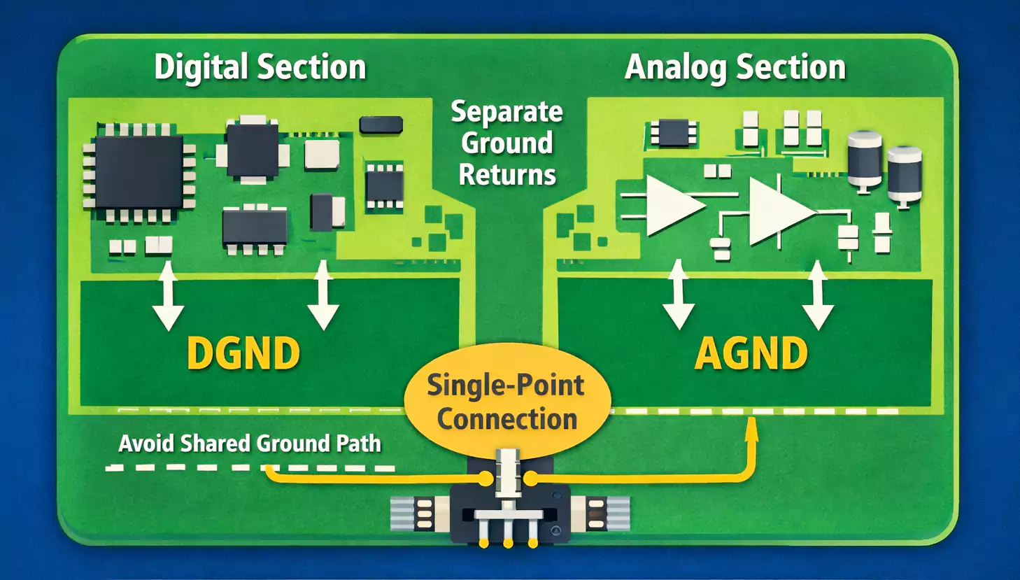
Return paths do the quiet work. Fast edges follow the lowest inductance path under the trace. A solid, continuous reference plane under high-speed routes keeps that loop small. Routing across a split plane, a slot, or an unstitched domain boundary forces the return around the gap and radiates. On two-layer boards, dedicating one side as much as practical to a continuous ground reference still helps; on multilayers, sandwiching susceptible traces between solid references reduces both radiation and pickup. Keep high-frequency paths short. Separate power and ground domains when circuits truly operate in different frequency regimes, and when analog and digital grounds must split, join them at one intentional common point rather than spraying accidental bridges across the board.
Voltage and spacing still matter for coupling and withstand. Yield-minded clearance grows with voltage difference; fabricator capability tables and IPC-style spacing guidance exist so etch yield and creepage stay honest. Trace/space margins that sit comfortably above the fab minimum (industry talk often treats roughly 6 mil class as a safer production comfort zone than pushing every net to the absolute process floor) buy etch yield without changing the schematic. Solid return copper plus disciplined spacing is cheaper EMI control than adding cans after the chamber fails.
Copper as the first heat path
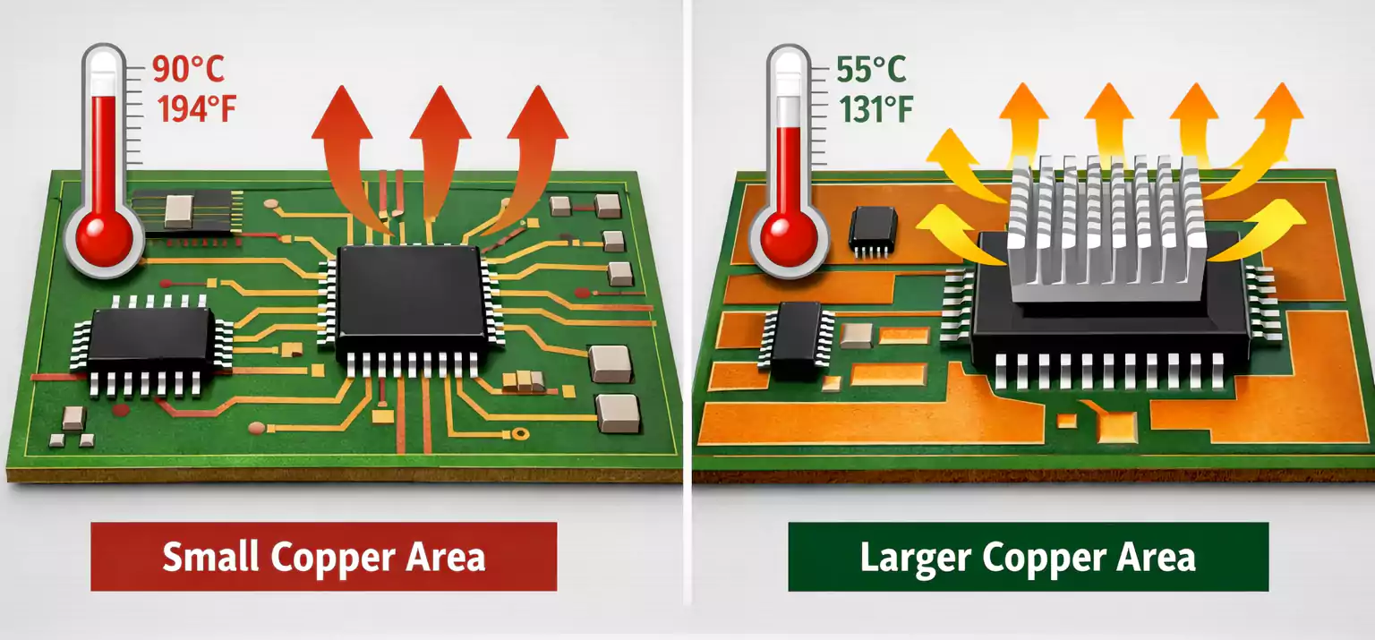
As density rises, temperature becomes a reliability driver long before a catalog heatsink appears on the BOM. Excess heat shifts parameters, shortens life, and creates the hotspots thermal cameras find after the electrical fixture said pass.
Use copper area as a heat spreader first. Pours around high-dissipation parts -- especially tied into ground copper with thermal vias into internal planes -- distribute heat and cut local peaks. Wider traces and heavier copper on power paths reduce both I2R heating and thermal gradients. Mesh-style internal grounds and edge-aware placement can help multilayer boards share heat and stay mechanically stable, but the principle is simple: give heat a copper path before you bolt on hardware.
Mechanical help still has a place. High-dissipation packages may need stand-offs, thermal interface material, or a heatsink when copper alone cannot meet the enclosure budget. Flame-retardant and higher-temperature laminates matter when process or ambient temperatures demand them. The expensive mistake is discovering the hotspot in pilot, then respining for copper pours and via arrays that should have been frozen with placement. Thermal design that starts after enclosure CAD is locked is how rework and late heatsink brackets enter the schedule.
Freeze these choices before the RFQ
Rework after a green electrical test usually traces to decisions that were still soft at quote time. Freeze package families and pad geometries against the real assembly process window, including fine-pitch caution and small-passive pad balance. Freeze laminate Tg, CTE expectations, thickness, and flatness needs against the thermal and reliability profile of the product. Freeze EMI zoning, reference continuity, and spacing margins so return paths and crosstalk budgets are intentional. Freeze copper heat paths and thermal-via strategy under power parts before enclosure and heatsink assumptions harden.
Send XFPCB an RFQ package that states those freezes in fab language: BOM with package callouts, stackup or material notes, fab and assembly notes for finish and via treatment, and Gerbers or ODB++ aligned to one revision. Annular ring and via aspect ratio still belong in that package as capability language -- enough ring after drill tolerance, aspect ratio the plating line can fill -- even when this article is not a full DFM checklist. Boards that pass electrical and then fail AOI, EMI, or thermal in pilot almost always deferred one of these freezes. Lock them early and the first production-minded spin stops being a rework fund.