
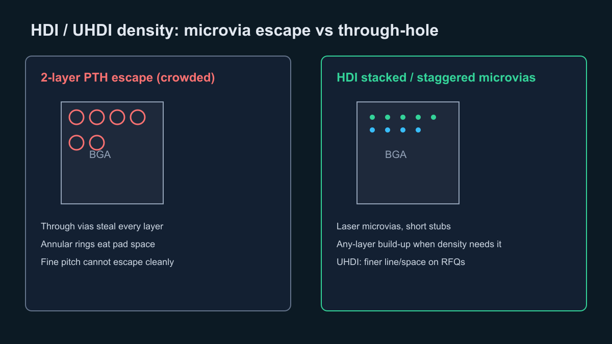
The RFQ still said "2-layer FR-4, 1 oz, HASL" while the layout already needed 0.4 mm-pitch BGA escape. CAM returned the same engineering question every China fab asks in that case: through-hole vias will not clear the pin field without stealing every layer and blowing annular-ring budget. The buyer was not wrong about cost discipline. The product had already moved past the construction that quote assumed.
Procurement and product leaders keep asking which PCB "trends" are real volume work and which stay science projects. From the fab floor the answer is blunt. Density (HDI / UHDI), form-factor flex and rigid-flex, materials that follow that density, and denser SMT process control are what show up as line items on RFQs. Market-size slides and lab demos that never clear CAM stay off the traveler.
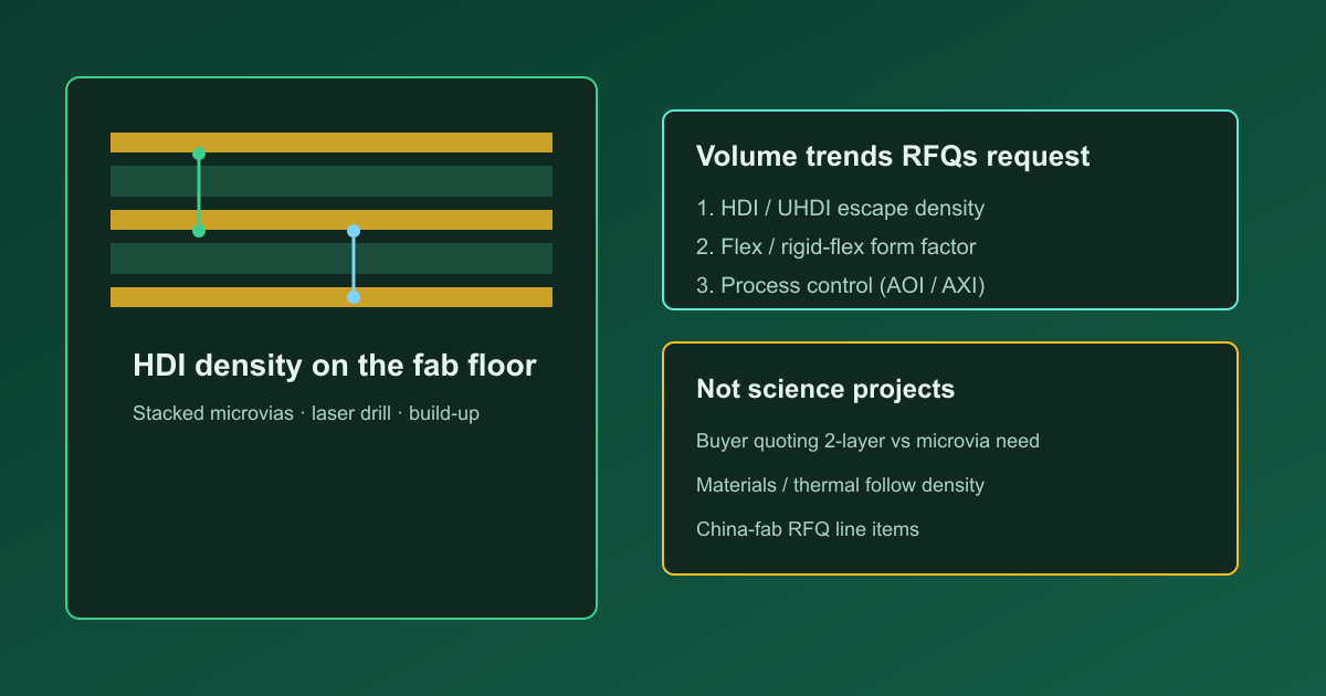
Density is the volume trend: HDI and UHDI
Fine-pitch packages, short high-speed stubs, and board outlines that refuse to grow force interconnect density up. That is HDI in the IPC sense: microvias, blind and buried structures, finer line and space, and higher connection density per area than a conventional through-hole multilayer menu.
What China fabs see moving in volume:
- Laser-drilled microvias with low aspect ratio (often near 1:1 or better) so plating fills reliably.
- Staggered and stacked microvia builds for sequential breakout under BGAs.
- Any-layer HDI when every dielectric interface must be available for escape -- not as a slogan, but when pin count and pitch leave no through-via path.
- UHDI-class fine line and space (tens of microns) on RFQs that used to accept coarser etch windows.
Through-hole still wins when density allows it. The trend that hits the traveler is when a 2-layer or single-lamination multilayer quote cannot escape the part without laser build-up. Embedded components exist in niche high-integration builds; they are not a default catalog SKU for most commercial RFQs. Treat them as a construction conversation after HDI escape and SMT density are already justified.
Flex and rigid-flex when form factor beats the harness
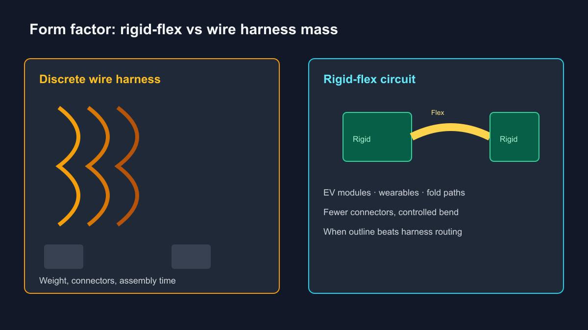
Flexible and rigid-flex constructions move volume when the product outline, weight, or folding path beats a discrete wire harness -- not because "flex is trendy." Wearables, medical patches, foldable consumer modules, and EV / mobility electronics that must drop connectors and harness mass are the usual drivers. Rigid islands hold BGAs and connectors; polyimide flex spans the bend and replaces cable assemblies that fail vibration or assembly takt time.
China-fab reality checks that keep flex out of science-project territory:
- Static bend versus dynamic flex class must be named on the drawing (cycle count and bend radius).
- RA copper and adhesiveless constructions matter for dynamic life; cheaper stacks fail early in the field.
- Coverlay, stiffener, and EMI shield stack-ups change yield and cost more than the copper count alone.
- Rigid-flex sequential lamination and coverlay registration are paid process steps -- quote them as such.
If the board never bends and never replaces a harness, rigid multilayer remains the cheaper, more available answer. Form factor is the filter.
Materials and thermal follow density -- they never lead it
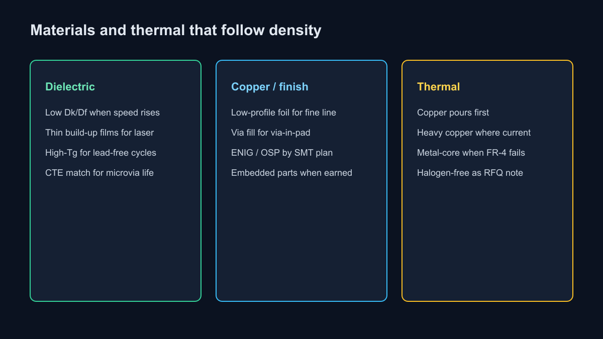
Low-Dk / low-Df laminates, high-Tg FR-4, thin build-up films, low-profile copper foils, and metal-core or heavy-copper options show up after density and power density force them. Buyers who start with a specialty laminate SKU before locking BGA pitch, impedance, and via type often over-buy materials while under-specifying the construction that actually fails CAM.
Practical sequencing that matches fab menus:
- Lock package pitch, layer roles, and via types (through vs laser vs sequential).
- Set dielectric heights and copper weights against impedance and thermal copper needs.
- Choose resin system (standard FR-4, high-Tg, low-loss, halogen-free) to match reflow cycles, CAF risk, and signal loss -- not a brochure claim.
- Escalate to metal-core or heavy copper when FR-4 copper pours cannot move the heat.
Sustainability themes that already appear as RFQ notes -- halogen-free laminates, RoHS finishes, closed-loop wastewater expectations at the supplier -- are process and material compliance items. They are not a substitute for stackup engineering.
AI and AOI as factory process change
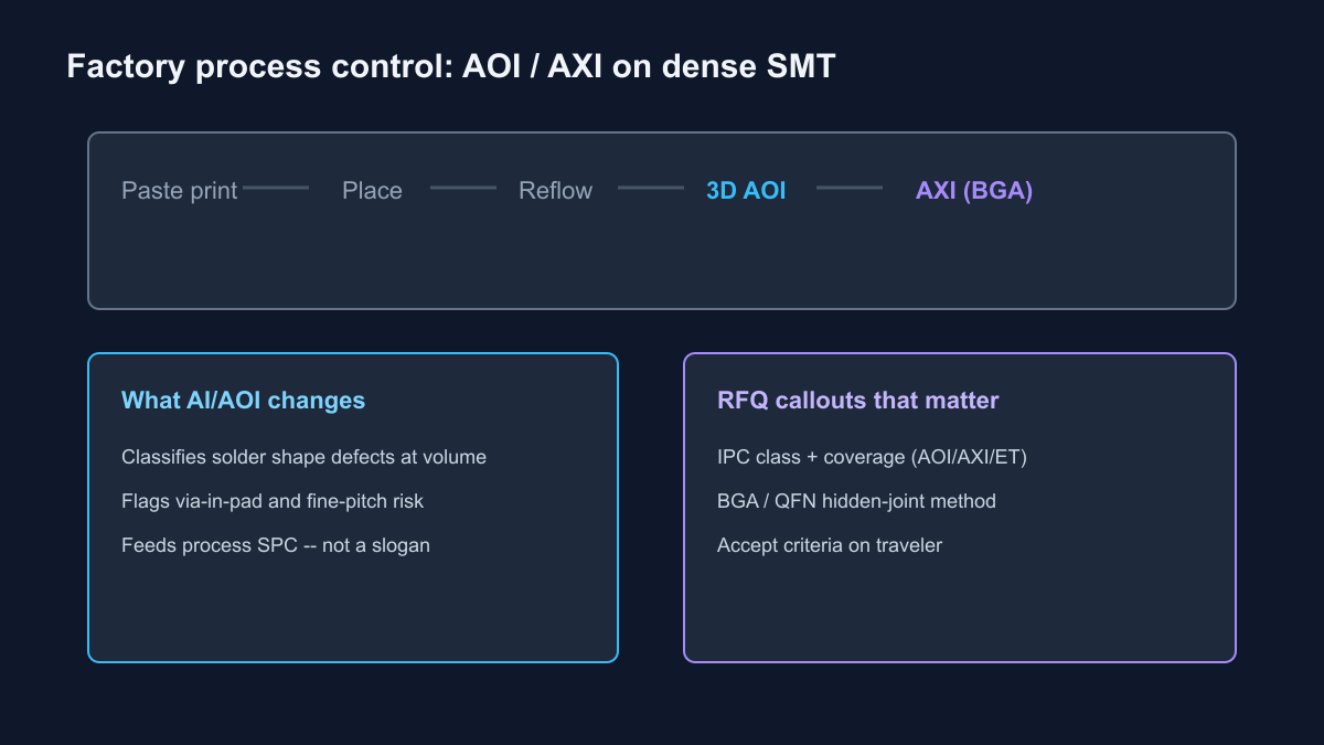
"AI in PCB" on marketing pages often means nothing a traveler can check. On the floor it means classification models and 3D AOI / AXI recipes that keep pace with denser SMT: finer paste apertures, via-in-pad, 01005 passives, and hidden joints under BGA and QFN. Defect images feed SPC and recipe tweaks. Predictive maintenance on placement and reflow equipment reduces unplanned stops. That is process control, not a product feature on the finished board.
What buyers should put on the RFQ instead of buzzwords:
- IPC class and which nets or packages need AOI, AXI, flying probe, or ICT.
- Accept criteria for voiding or solder shape when BGA/QFN are in play.
- Whether first-article includes X-ray sampling and how that maps to production coverage.
Lab additive / 3D-printed circuit demos and exotic SoC print claims remain outside mainstream China fab capacity for production RFQs. Quote laser HDI, sequential lamination, and qualified SMT inspection first.
When a trend becomes an RFQ line item
China fabs price what is written. If the product needs microvia escape, flex bend class, low-loss dielectric, or AXI coverage, those must be line items -- not footnotes in an email thread.
Ask the fab explicitly:
- HDI type: 1+N+1, 2+N+2, or any-layer; laser via diameter and fill; staggered vs stacked; minimum line/space and annular ring.
- Flex / rigid-flex: static vs dynamic, bend radius, copper type, coverlay / stiffener / shield, and fold locations dimensioned.
- Materials: Dk/Df or loss class if SI-critical, Tg, halogen-free, copper foil type (standard vs low-profile), finished thickness and tolerance.
- Thermal: copper weight, metal-core yes/no, thermal via arrays called out on the drawing.
- Assembly and inspection: IPC class, AOI/AXI/ET coverage, via-in-pad fill and cap, surface finish matched to the reflow plan.
Send one revision-aligned package: Gerbers or ODB++, drill, stackup drawing, fab notes, and -- if assembly is in scope -- BOM, centroids, and AVL rules. Ambiguous "HDI preferred" language produces quotes that cannot be compared and CAM holds that burn schedule.
XFPCB quotes from that package so density, form factor, materials, and inspection coverage match the product you are actually releasing -- not a 2-layer habit left over from the last generation.
Trends that hit the fab floor are constructions and process controls a traveler can run: HDI density for escape, flex when outline beats harness, materials and thermal that follow those choices, and AOI/AXI coverage for denser SMT. Write them as RFQ line items. Leave market-size hype and lab demos off the traveler.