
The PCB design engineer’s manufacturing job is not “make the schematic look pretty in CAD.” It is to own manufacturable intent between schematic vision and the fab traveler: stackup and class callouts, Gerber/BOM discipline, impedance notes CAM can price, and a release package that survives first-pass DFM without a week of engineering questions (EQ). Soft-skills marketing about “collaboration culture” does not open a panel. Files, notes, and locked assumptions do.
This China-fab view answers first: what CAM actually opens on day one, how DFM differs from a green DRC report, which EQ themes burn schedule, when to pull the fab in early (HDI, controlled impedance, Class 3, flex), and how buyers and design engineers should split RFQ work so quotes are comparable. Layout depth: PCB board design layout considerations. DFM checklist companion: PCB DFM (design for manufacturing). Process background: how PCBs are made.
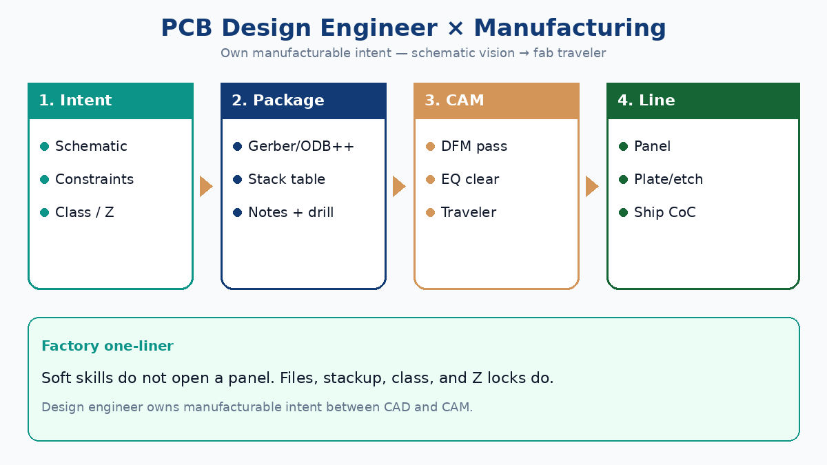
Answer first: manufacturable intent, not film-director fluff
| Soft marketing claim | What the fab traveler actually needs | Owner on the customer side |
|---|---|---|
| “Cross-functional collaboration” | Complete Gerber/ODB++ + drill + netlist + fab notes | Design engineer (package) + buyer (PO locks) |
| “Design leadership” | Stackup table, copper weight, Tg/material family | Design engineer |
| “Attention to detail” | Class, finish, impedance method, hole chart | Design engineer on drawing; buyer on RFQ line 1 |
| “Stakeholder alignment” | One revision set — no mixed Gerber vs BOM rev | Design engineer + document control |
One-line definition: The design engineer translates electrical intent into geometry, stack, and notes a China CAM desk can price and build without inventing defaults. If those defaults are wrong, you pay in EQ loops, respin, or silent Class 2 habit on a Class 3 hope.
💡 Procurement Pro-Tip: Ask engineering for the release package checklist (next section) before you send the RFQ. A beautiful schematic PDF without stackup, class, and netlist is not a fab package — it is a brainstorming artifact.
Related buyer vocabulary: PCB terminology for buyers. Tooling context (without turning this into a CAD review): PCB design software programs.
Release package checklist CAM actually opens
CAM does not “feel” your design intent. They open files and look for contradictions. Ship this set as one revisioned zip (or ODB++ job) with a fab drawing / notes PDF.
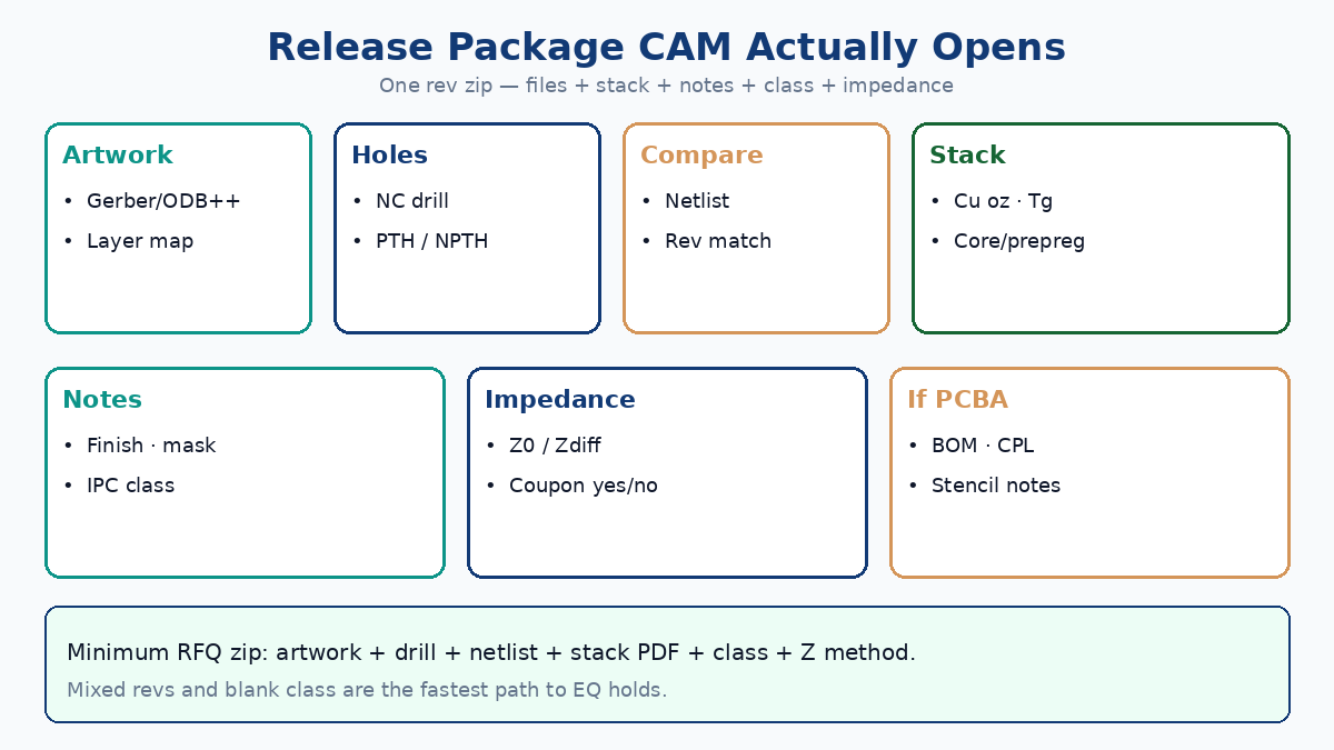
| Deliverable | What “done” looks like | Typical fail if missing |
|---|---|---|
| Gerber or ODB++ | Layer map matches filenames; soldermask/silkscreen sides clear | Wrong layer order; mask on wrong side |
| NC drill | PTH vs NPTH separated; plated slots called out | NPTH plated by habit; slot quotes wrong |
| IPC-356 / netlist | Matches copper for compare | Silent opens/shorts found after etch |
| Stackup table | Layer count, core/prepreg, Cu oz, Tg / material family | “FR-4 equivalent” → bidder roulette |
| Hole chart | Finished sizes, tolerance, aspect notes | Drill house invents tolerance |
| Fab notes | Finish, solder mask color, legend, IPC class | Defaults to cheapest commercial habit |
| Impedance block | Z0/Zdiff, layer, tolerance, coupon/TDR yes-no | “Impedance capable” brochure pricing |
| BOM + AVL (if PCBA) | MPN, alternates, DNP flags, rev match | Wrong kit; polarity scrap |
| Readme / rev | Single rev letter for all files | Mixed revs → EQ stop |
Minimum China RFQ zip: Gerber (or ODB++) + drill + netlist + stackup PDF + fab notes with IPC class and impedance method. Everything else is optional until PCBA or special process enters scope.
Naming that CAM trusts: Use a single job name and rev in every filename (JOB_R02_GTL.gbr, not final_final2). Put a one-page readme with layer map, units (inch/mm), and contact for EQ. ODB++ jobs still need the same notes content — format does not replace stackup, class, or Z locks.
PCBA add-ons: When assembly is in the same RFQ, add CPL (XY, rotation, side), paste/stencil aperture notes, and polarity-critical MPN callouts. Fab-only packages that suddenly become turnkey without CPL are a classic first-paste scrap path.
⚠️ Watch Out for: Shipping Gerbers from one rev and a BOM from another, or pasting “impedance controlled” in email without layer/target/tolerance. CAM will stop the job or price the safe (expensive) interpretation.
Typical EQ themes — and how designers cut the loops
Engineering questions are not personal criticism. They are missing locks. The same themes dominate China fab EQ queues.
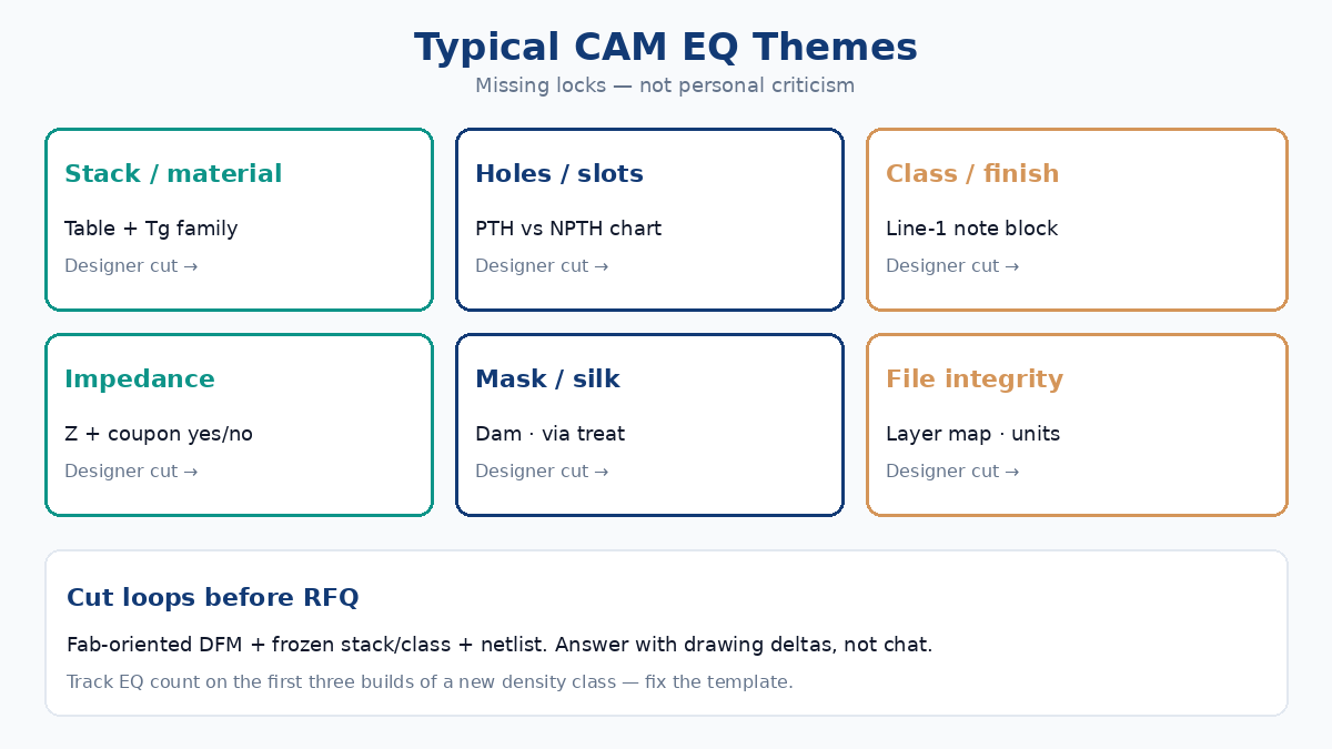
| EQ theme | What CAM is really asking | Designer cut that works |
|---|---|---|
| Stack / material | Which core/prepreg and Tg are contractual? | Publish a stack table; name family or approved equivalents |
| Holes / slots | PTH vs NPTH? Plated slot? Tolerance? | Hole chart + NPTH layer or explicit note |
| Annular ring / pads | Will Class X survive drill wander? | Size pads to stated class before release |
| Impedance | Model-only or coupon/TDR? Which layers? | Z block on drawing; coupon yes/no on RFQ |
| Class / finish | Class 2 default vs your Class 3 hope? | Class + surface finish on note block line 1 |
| Mask / silk | Over copper? Cover vias? Min dam? | Mask expansion / via treatment notes |
| File integrity | Layer map, units, mirror, missing paste | One package + layer list in readme |
How to cut loops before RFQ: run a fab-oriented DFM (not only CAD DRC), freeze stack and class early, and attach the netlist. Most multi-day EQ storms start from blank class, vague FR-4, or Gerber-only dense multilayers.
Response discipline: Answer with drawing deltas (rev, note number), not chat paragraphs. If CAM proposes an equivalent stack, approve or reject in writing with Dk/Df and thickness implications for impedance. Silence is not approval — travelers assume the cheapest unread option.
Metric that matters: Track EQ count and days-to-clear on the first three China builds of a new density class. If you still see five-plus EQ themes after package discipline, the rule deck or stack template is wrong — fix the template, not only the one job.
Process companion when EQ asks “can we even build this stack?”: how PCBs are made. DFM gates: PCB DFM.
DFM vs DRC: green DRC ≠ fab-ready
| Check | What it proves | What it does not prove |
|---|---|---|
| DRC (CAD) | Geometry obeys your rule deck (clearance, width, via sizes you set) | Fab can plate, register, and yield at their process window |
| DFM (fab) | Design fits drill, etch, mask, plating, and class capability for a plant | Your schematic intent is electrically optimal |
| Green DRC report | No violations against local constraints | Annular ring for Class 3, aspect ratio, mask dam, impedance stack |
A board can pass DRC with 3 mil clearance and still fail China DFM when the chosen fab’s standard window is 4 mil, or when Class 3 annular ring was never in the rule deck. DRC is necessary; DFM is release-gating.
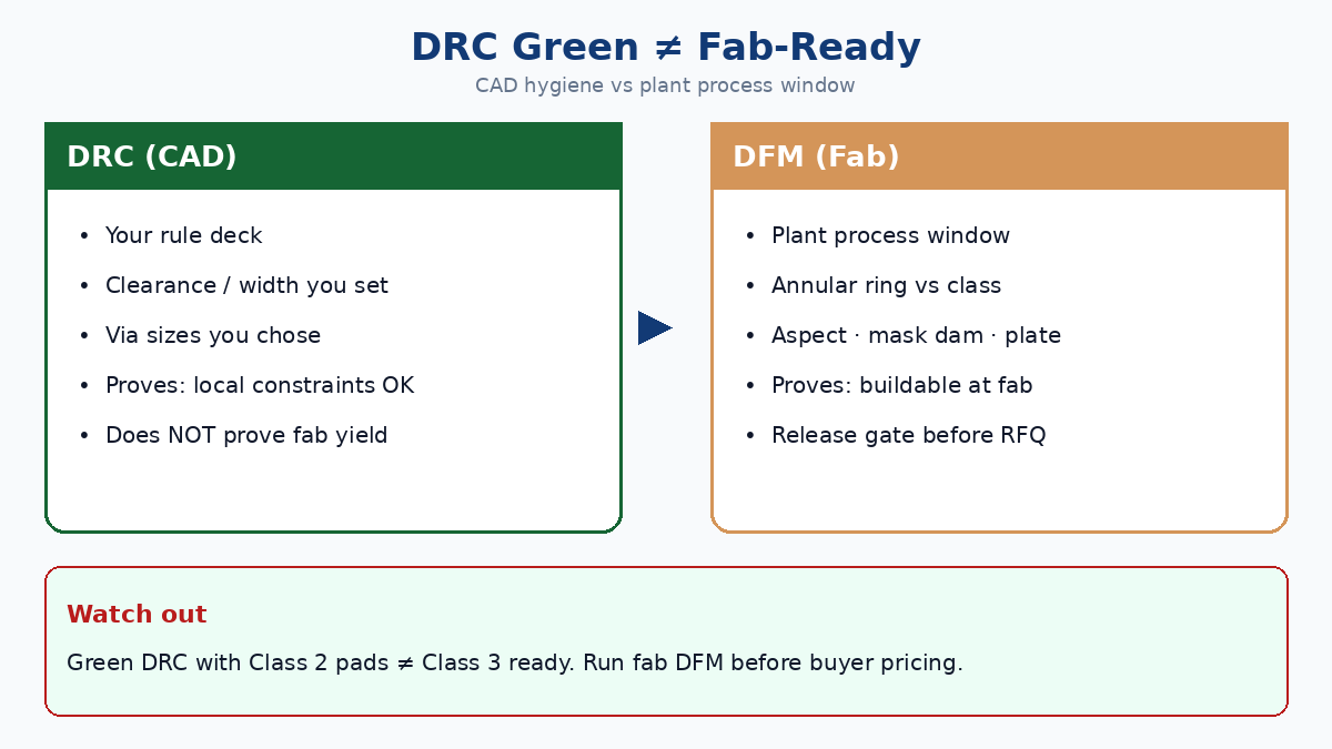
What to put in the designer’s DFM pass before buyer RFQ: min trace/space vs stated fab capability, annular ring vs stated IPC class, aspect ratio on smallest PTH, solder-mask dam on finest pitch, copper balance / thieving notes if the fab requires them, and impedance stack consistency with the Z block. If any item is “unknown,” the package is not release-ready.
Practical release rule: Treat CAD DRC as the designer’s hygiene. Treat fab DFM (or an early CAM review on HDI/Z/Class 3/flex) as the gate before buyer pricing. Do not tell procurement “it’s clean” because the DRC light is green.
💡 Procurement Pro-Tip: On first RFQ for a new density class, ask for a written DFM result (pass / conditional / fail) with the quote — not a verbal “looks fine.” Conditional DFM is where real cost hides.
Layout habits that feed DFM: PCB board design layout considerations.
When to involve the fab early
Pull CAM/application engineering in before artwork freeze when any of these are true. Waiting until RFQ day turns early advice into late EQ.
| Trigger | Why early fab help pays | What to send for a 30-minute review |
|---|---|---|
| HDI / microvia / via-in-pad | Stack and via architecture drive yield and NRE | Draft stack, via types, min pitch |
| Controlled impedance | Material Dk/Df and construction change Z | Target Z0/Zdiff, layer intent, coupon plan |
| IPC Class 3 | Pads and plating must be sized up front | Class callout, critical pad/hole list |
| Flex / rigid-flex | Bend, coverlay, and stiffener rules are plant-specific | Stack sketch, bend areas, finish |
| Unusual thickness / aspect | Plateability and drill wander | Thickness, min drill, aspect estimate |
| Tight mask dam / fine pitch | Bridging and registration risk | Pitch, dam targets, finish |
Do not involve fab early for every two-layer LED board with generous clearances — that burns application bandwidth. Do involve them when a respin would cost more than a week of chat.
Timing tip: Book the review when the stack and critical pitch are 80% frozen — early enough to change copper, late enough that CAM is not guessing from a napkin. Bring the same checklist you will put on the RFQ so advice becomes notes, not folklore.
⚠️ Watch Out for: “We’ll fix Class 3 / impedance in ECO after prototype.” Stack and pad geometry rarely survive a late class upgrade without copper changes. Lock class and Z method at architecture, not at PO panic.
Buyer / engineer RFQ collaboration matrix
Quotes go sideways when buyers negotiate price while engineers still negotiate intent. Split ownership explicitly.
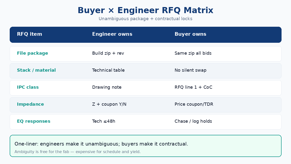
| RFQ item | Design engineer owns | Buyer owns | Shared lock |
|---|---|---|---|
| File package completeness | Build zip + rev | Attach same zip to all bidders | One rev letter |
| Stackup / material | Technical table | “No silent material swap” on PO | Approved equivalents list |
| IPC class | Drawing note | Line-1 RFQ + CoC language | Same class on drawing and PO |
| Impedance | Z block + coupon yes/no | Price coupon/TDR as line item | Method identical across bidders |
| Lead time / qty / Incoterms | Feasibility flag if crazy | Commercial terms | Realistic FA date |
| Alternates / AVL | Engineering approve | Cost negotiate within AVL | Written AVL, not verbal |
| EQ responses | Technical answers ≤24–48h | Chase and log holds | Single EQ mailbox / thread |
Matrix one-liner: Engineers make the package unambiguous; buyers make the package contractual. Ambiguity is free for the fab and expensive for you.
Soft next step
If you are releasing a multilayer, impedance, Class 3, or HDI job to China, send the release checklist and class/Z locks with the first RFQ — not after the first EQ storm. XFPCB works from drawing-driven packages: stackup, class, and notes on the traveler, not soft-skills slogans. Pair this page with PCB DFM, layout considerations, and how PCBs are made when design and process need one handoff story.