
Overseas PCB buyers and technicians lose money when quote language and CAM EQ questions mean different things to purchaser, design, and the China fab. A long A–Z dictionary helps search; it does not tell you which words move price, yield, or schedule if you leave them vague. This guide is answer-first and grouped by quote impact: file-package terms, stackup and material, geometry, impedance and IPC class, PCBA inspection words, and a mini RFQ checklist of must-lock fields. Use it beside the support glossary for definitions, then lock the commercial meanings on the RFQ.
Companion support page (definitions, not this buyer map): PCB terminology glossary. Process and DFM depth: how PCB assembly works, PCB DFM, IPC Class 3 PCB fabrication, controlled impedance custom PCBs.
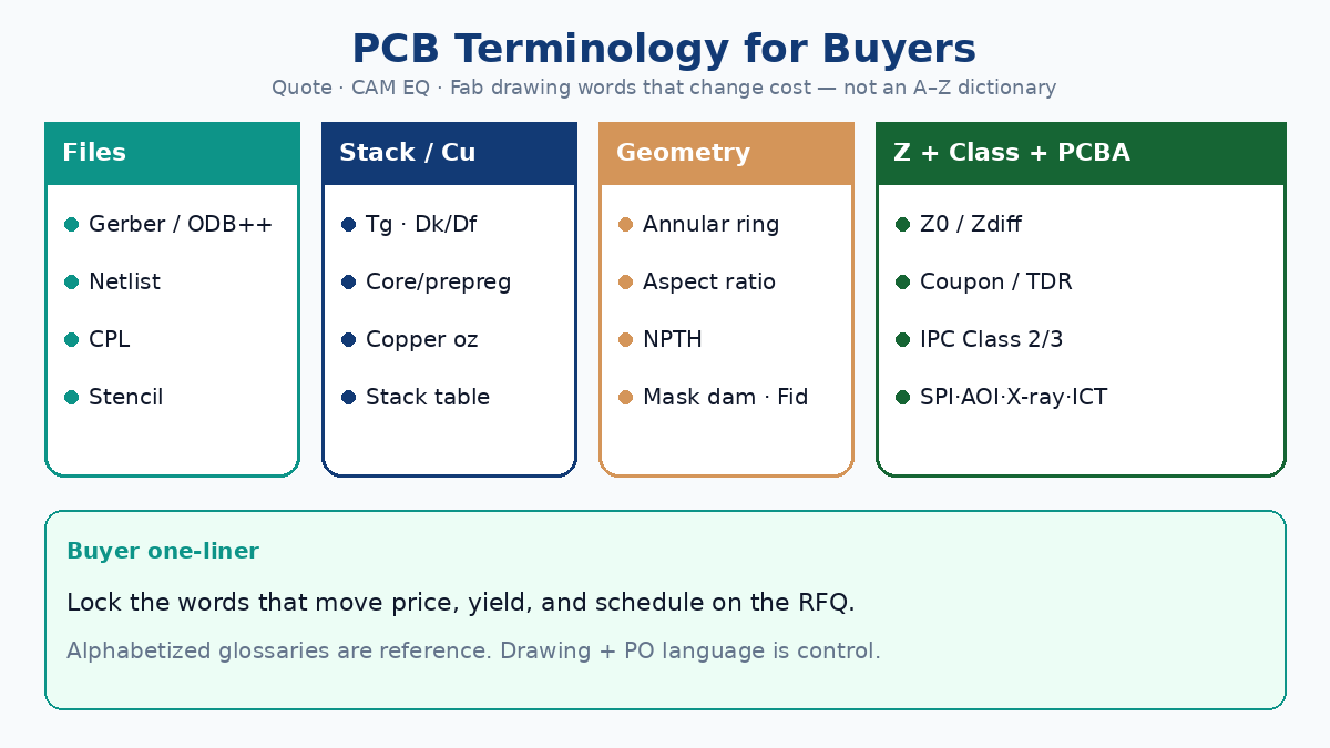
Answer first: which terms move price and yield
| Term cluster | What CAM / sales hear | What buyers often meant | Cost / yield hit if mismatched |
|---|---|---|---|
| File package | Gerber vs ODB++, netlist, CPL, stencil aperture | “Send Gerbers” | Wrong apertures, polarity scrap, EQ loops |
| Stackup / material | Tg, Dk/Df, core vs prepreg, copper oz | “FR-4 is fine” | Impedance miss, delam risk, material upcharge |
| Geometry | Annular ring, aspect ratio, NPTH, mask dam, fiducial | “Same as last rev” | Drill scrap, solder bridges, placement fail |
| Impedance / class | Z0/Zdiff, coupon/TDR, IPC Class on drawing | “Controlled impedance / high reliability” | Model-only quotes, Class 2 default, FA fights |
| PCBA gates | SPI, AOI, X-ray, ICT, turnkey vs consignment | “Full inspection” | Brochure coverage, kit ownership fights |
One-line definition: Buyer terminology that matters is the set of words that appear on quotes, CAM EQ emails, and fab/assembly drawings — and that you can enforce at receiving. Alphabetized lists are reference; RFQ locks are control.
💡 Procurement Pro-Tip: Before you chase a lower unit price, ask: which three terms on this RFQ, if misunderstood, would force a respin or a Class downgrade? Lock those first. Everything else is secondary.
File package terms (Gerber, ODB++, netlist, CPL, stencil)
CAM cannot price or build what the package does not define. Incomplete files create “capacity” delays that are really data gates.
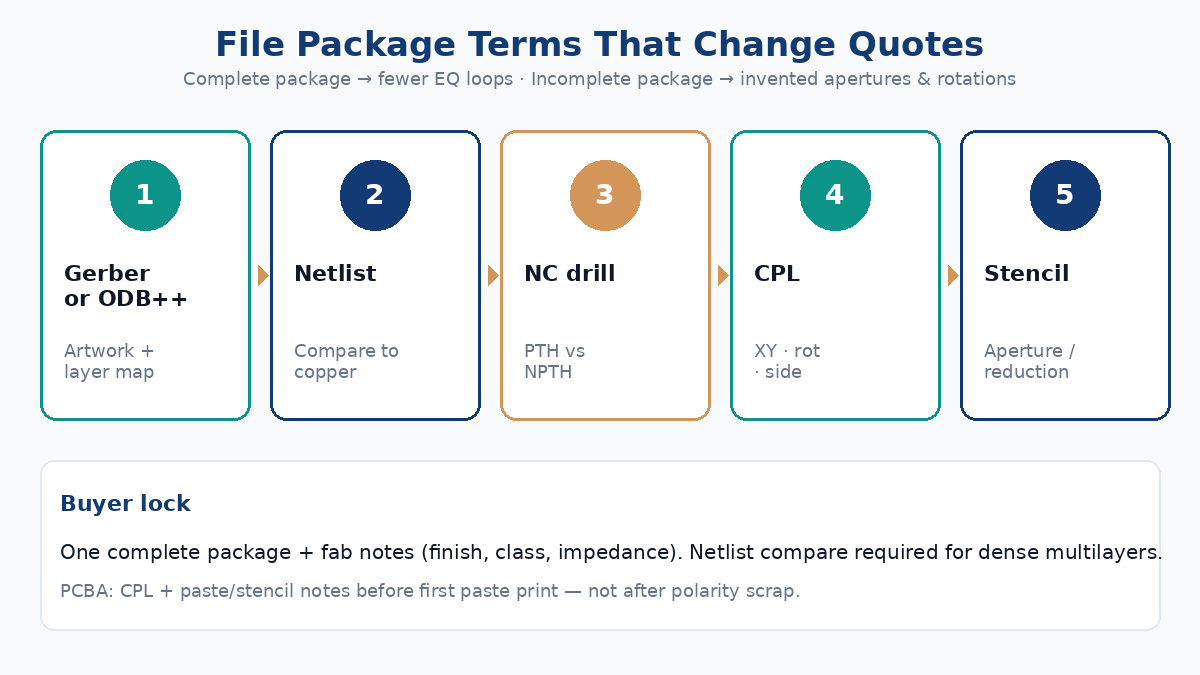
| Term | Shop meaning | Lock on RFQ / drawing | Fail mode if vague |
|---|---|---|---|
| Gerber (RS-274X) | Layer artwork + apertures for etch/mask/silk | Layer map, units, polarity, board outline | Missing mask or wrong polarity → scrap |
| ODB++ / IPC-2581 | Intelligent package (often preferred for complex stacks) | Format + revision; still add fab notes | Assumed “same as Gerber” when stack differs |
| Netlist (IPC-356) | Connectivity truth for CAM compare | Require netlist compare vs Gerber | Silent opens/shorts until ET or field |
| NC drill | Tool sizes, PTH vs NPTH, plated slots | Separate PTH/NPTH; plated slot callouts | NPTH plated by habit; wrong hole chart |
| CPL / centroid | XY, rotation, side for pick-and-place | Rotation convention + side; match BOM rev | Polarity flips; “manual guess” quotes |
| Stencil aperture | Paste opening vs pad (often reduced) | Home-plate / step-stencil notes for fine pitch | Excess/insufficient paste; SPI fails later |
Gerber vs ODB++ (buyer rule): Either can work. What fails is a partial Gerber set without a layer map, or ODB++ without written fab notes for finish, impedance, and class. Prefer one complete package plus a one-page fab note block.
Netlist: Ask CAM to compare netlist to copper. “We imported Gerbers” is not a compare. Dense multilayers without netlist compare are how EQ misses become ET escapes.
CPL and stencil: Assembly quotes that omit CPL and paste rules invent rotations and apertures. For fine pitch (~0.5 mm and below) and micro-BGA, write stencil reduction and SPI expectation on the RFQ — not after first article.
⚠️ Watch Out for: “Gerber only” PCBA quotes on mixed SMT+THT boards. Without CPL and an assembly drawing, two plants invent different rotations and THT methods, then argue about polarity scrap after the PO.
Stackup and material (Tg, Dk/Df, core/prepreg, copper oz)
Material language changes both fab cost and electrical behavior. “FR-4 equivalent” is not a stackup.
| Term | Shop meaning | Why quote moves | Buyer lock |
|---|---|---|---|
| Tg (glass transition) | Softening temperature of resin system | Mid/high-Tg upcharge; lead-free process window | Name Tg target or laminate family |
| Dk / Df | Dielectric constant / dissipation factor | Impedance and loss; specialty resins cost more | Dk/Df at frequency for Z-critical nets |
| Core | Cured laminate with copper (often) | Thickness library; availability | Core thicknesses in the stack table |
| Prepreg | B-stage resin glass used to bond layers | Resin content drives thickness after press | Prepreg types / count; not “fill as needed” |
| Copper weight (oz) | Starting foil weight (e.g. 1 oz ≈ 35 µm) | Etch time, impedance, thermal | Outer/inner oz separately; plating add-on separate |
| Stackup table | Layer-by-layer copper + dielectric map | Impedance model input; press recipe | Numbered layers, oz, dielectric, thickness |
Tg: Lead-free reflow and high-layer counts often need mid-Tg or high-Tg systems. Leaving Tg blank lets CAM pick the cheapest FR-4 that fits the press — fine for many consumer boards, risky for thermal or CAF-sensitive designs.
Dk/Df: Controlled-impedance and high-speed buyers must lock dielectric identity or Dk at the design frequency. “Impedance 50 Ω” with no stack and no material is a modeled hope, not a fab contract. Depth: controlled impedance custom PCBs.
Core vs prepreg: Buyers who only state finished thickness force CAM to invent core/prepreg combinations. That invention may hit impedance and registration differently than your CAD model. Send the stack table you used for Z-calc.
Copper oz: Outer 1 oz vs 2 oz changes etch factor and min trace/space. Inner 0.5 oz vs 1 oz changes impedance and plane thermal mass. Write outer and inner separately; do not treat plated finished copper as the same as foil weight.
💡 Procurement Pro-Tip: Paste your stackup table (layer, copper oz, dielectric type, thickness) into every RFQ. Two fabs quoting “1.6 mm FR-4” without the same table are not comparable.
Geometry terms (annular ring, aspect ratio, NPTH, mask dam, fiducial)
These words decide drill yield, solderability, and whether SMT can place at all.
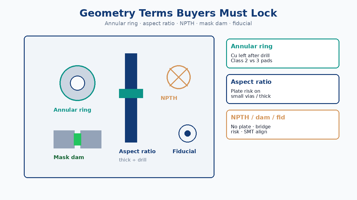
| Term | Shop meaning | Typical buyer miss | Cost / scrap path |
|---|---|---|---|
| Annular ring | Copper ring remaining around a drilled hole after fabrication | Pad drawn for Class 2 habit; Class 3 expected | Breakout, scrap, or forced pad growth |
| Aspect ratio | Board thickness ÷ drill diameter (PTH) | Tiny vias in thick boards | Plating voids; Class fails; forbids drill size |
| NPTH | Non-plated through hole (no copper in barrel) | Mechanical holes left in PTH layer | Unwanted plating; press-fit / screw issues |
| Solder mask dam | Mask web between adjacent pads / openings | Fine-pitch pads with zero dam | Bridging; forced mask-defined redesign |
| Fiducial | Optical target for SMT alignment | Missing global/local fids on panel | Placement offset; AOI noise; line refuse |
Annular ring: Quoting IPC Class without checking pad vs drill is how Class 3 programs fail DFM. Fix pads on the drawing; do not hope CAM “makes ring somehow.” See IPC Class 3 PCB fabrication.
Aspect ratio: High ratio (thick board, small drill) raises plating difficulty and scrap. Ask CAM for max aspect ratio on your thickness before you freeze via size.
NPTH vs PTH: Mark mechanical holes, tooling slots, and press-fit cavities clearly. Silent PTH plating on an NPTH ruins fits.
Mask dam: Fine-pitch QFP/QFN need a minimum dam. If your paste and mask openings leave zero web, expect bridges or a CAM EQ that widens openings against your intent.
Fiducials: Global panel fids plus local fids near fine-pitch / BGA sites are assembly insurance. Cheap boards without fids look fine in photos and fail placement yield.
Related layout discipline: PCB DFM.
Impedance and class (Z0/Zdiff, coupon/TDR, IPC Class 2/3)
“Controlled impedance” and “Class 3” are the two phrases that most often appear on marketing slides and disappear from the traveler.
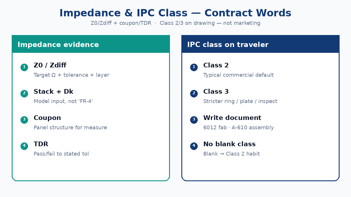
| Term | Contractual meaning | Vague substitute to avoid | Enforce with |
|---|---|---|---|
| Z0 / Zdiff | Single-ended / differential target ohms + tolerance | “High-speed layout” | Stack + trace/space + reference plane + material |
| Coupon | Test structure on panel for impedance (and plating) | “We control impedance in process” | Coupon design + which nets represented |
| TDR | Time-domain reflectometry measurement of coupon/trace | “Modeled OK” | TDR report to stated tolerance |
| IPC Class 2 / 3 | Acceptance/performance class on fab (e.g. IPC-6012) and/or assembly (IPC-A-610) | “High reliability” | Class number + document + revision on drawing/PO |
Z0 / Zdiff: Lock target, tolerance (e.g. ±10%), layer, and reference. Without stack and material, fabs quote “impedance capable” — meaning they can run coupons when you pay for them, not that your design is already controlled.
Coupon / TDR: Model-only impedance is free; coupon + TDR is evidence. For production Z-critical boards, require coupons and a pass rule. For early prototypes, you may accept model-only — but write that choice so both bidders price the same.
IPC Class: Class is a drawing and PO acceptance level, not a factory badge. Blank class → Class 2 defaults are common in China. Class 3 without annular ring and plating callouts is incomplete. Full map: IPC Class 3 PCB fabrication.
⚠️ Watch Out for: Citing “IPC Class 3” with no document family (6012 vs A-610) or citing A-610 Class 3 on a bare-board-only PO. Fab and assembly classes are related but not the same traveler.
PCBA terms (SPI, AOI, X-ray, ICT, turnkey vs consignment)
Assembly quotes hide large cost in inspection coverage and kit ownership. “Full inspection available” is brochure language.
| Term | What the line does | When buyers should require it | RFQ lock |
|---|---|---|---|
| SPI | Measures paste volume/height before place | Fine pitch, micro-BGA, new stencil FA | Coverage % + package list |
| AOI | Optical inspect after reflow (and often more) | Default for production SMT | Side coverage; escape criteria |
| X-ray | Sees hidden joints (BGA, many QFN/LGA) | Hidden joints in scope | Sample vs 100%; refdes list |
| ICT | Bed-of-nails electrical test | Stable volume after fixture NRE | Fixture owner + coverage |
| Flying probe | Fixtureless electrical opens/shorts | NPI / low volume | Net coverage expectations |
| Turnkey | Plant buys parts (often fab too) | When AVL and substitutes are clear | AVL + substitute approval process |
| Consignment | You supply the kit | When you own inventory / controlled AVL | Kit readiness gate before paste |
SPI / AOI / X-ray: Tie methods to packages and pitch. Availability is not a traveler. Process map: how PCB assembly works.
ICT vs flying probe: Flying probe fits NPI; ICT fits volume once fixture cost amortizes. Do not assume ICT is free or included in “test.”
Turnkey vs consignment: This is kit-risk language, not a quality grade. Turnkey needs written AVL rules; consignment makes you the bottleneck for short kits and MSL mistakes. Put the model on RFQ line 1.
Mini RFQ checklist — must-lock terms
Fill once; paste into every China fab/PCBA RFQ so bids stay comparable.
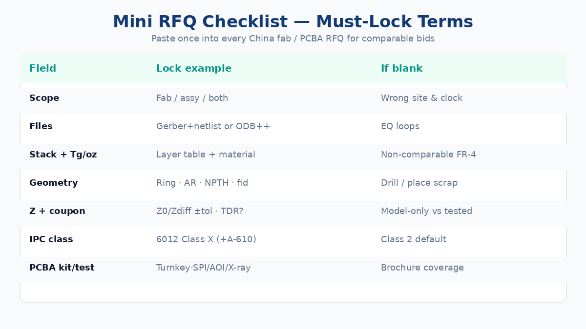
| Must-lock field | Example language | If you leave it blank |
|---|---|---|
| Scope | Fab only / assy only / fab+assy | Wrong site and lead-time clock |
| File set | Gerber+drill+netlist or ODB++; layer map | EQ loops; silent layer mistakes |
| Stackup + material | Table + Tg / laminate name + outer/inner oz | Non-comparable “FR-4 1.6 mm” bids |
| Geometry gates | Min annular ring, max aspect ratio, NPTH list, fiducials | Drill/mask/placement scrap |
| Impedance | Z0/Zdiff + tol + coupon/TDR yes/no | Model-only vs tested priced as same |
| IPC class | IPC-6012 Class X (+ A-610 if PCBA) | Class 2 default; FA disputes |
| Finish | ENIG / HASL / OSP + key thickness / age rules | Finish swap mid-build |
| PCBA kit model | Turnkey + AVL or consignment | Shortage ownership fights |
| Inspect / test | SPI/AOI/X-ray rules; ICT/FP/FCT ownership | Brochure “available” coverage |
| No silent change | No class/material/stack change without signed ECO | Traveler quietly cheapens |
Minimum viable buyer RFQ: scope + complete file set + stackup table + IPC class + finish + (if Z-critical) impedance method + (if PCBA) kit model and SPI/AOI/X-ray rules. Add annular ring and aspect notes when Class 3 or thick/thin extremes apply.
For alphabetized term lookup while you draft: PCB terminology glossary. For DFM before CAM: PCB DFM. For Z programs: controlled impedance custom PCBs. For Class 3 drawing language: IPC Class 3 PCB fabrication. For assembly traveler language: how PCB assembly works.
Soft next step
If overseas quotes keep shifting after CAM EQ, send the stackup table, hole chart, class line, and the checklist above in the first RFQ. XFPCB helps buyers and technicians lock quote and fab-drawing language before the traveler starts — clear terms on the PO, not a longer dictionary after scrap.