
HDI boards need microvias that a twist drill does not want to own. CO₂ laser drilling is the usual factory answer for ablating organic dielectric down to a copper stop so a blind microvia can be cleaned and plated. It is not a replacement for every hole on the panel, and it is not the same process as laser work on flex coverlay.
This post is the rigid-HDI process choice for overseas buyers and engineers: what CO₂ ablation actually stops on, what still belongs on a mechanical spindle, and what the stack note must say. No invented diameter floors, no machine brand list, and no claim that laser always beats a bit on cost.
What CO₂ laser drilling is doing
A CO₂ laser in the far infrared is absorbed well by organic dielectrics (FR-4 style resins, polyimide films used as HDI dielectrics). The beam heats and vaporizes dielectric. Copper reflects much of that wavelength, so a continuous copper pad or plane under the dielectric acts as a natural stop. That is why blind microvias that land on a capture pad are a natural CO₂ job after the dielectric is in place.
UV lasers (shorter wavelength) can machine copper as well as dielectric and are the usual tool when the process must open copper or push to smaller features than the CO₂ process window supports. Treat UV versus CO₂ as a process family choice on the quote—not as interchangeable names for “laser.”
Flex coverlay skive and windowing is a different traveler. Our flex laser-ablation guide owns that; this post stays on rigid HDI microvias.
Where it sits in an HDI sequence
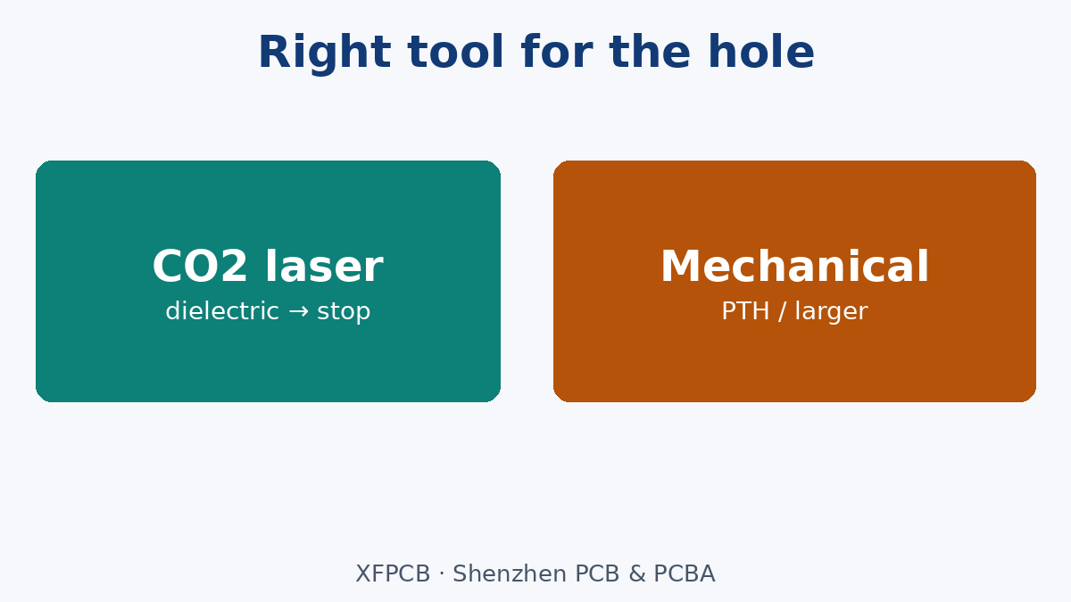
A typical HDI build uses sequential lamination: dielectric and copper added in steps, microvias drilled and plated, then the next dielectric. In that sequence CO₂ drilling usually happens after a dielectric is applied over a patterned copper stop, then desmear/debris clear, then copper metallization of the via. Stacked and staggered microvia architectures are stackup decisions first; laser is the tool that opens the dielectric for those vias. Our HDI PCB page is the construction family; the stack note must still name which layers are laser-drilled.
Strengths that matter on the RFQ
- Non-contact: no bit breakage in the microvia size range, no spindle vibration into a fragile outer build-up.
- Natural stop on copper when the capture pad is present and continuous under the shot.
- High via counts: many microvias per panel are often faster on laser than on a brittle micro-bit.
Limits you should write, not assume
Copper must be opened another way when the process needs a hole through copper. CO₂ is inefficient at removing copper. Conformal mask or a copper window (etch or UV) is part of many recipes before dielectric ablation. Say which recipe you expect.
Depth without a stop is harder. Blind depth into thick dielectric without a capture pad invites taper and depth scatter. Prefer a designed stop layer.
Aspect ratio and plating still govern reliability. A clean laser hole that is too deep for the diameter will still plate poorly. Continuity test does not prove plating thickness on the wall.
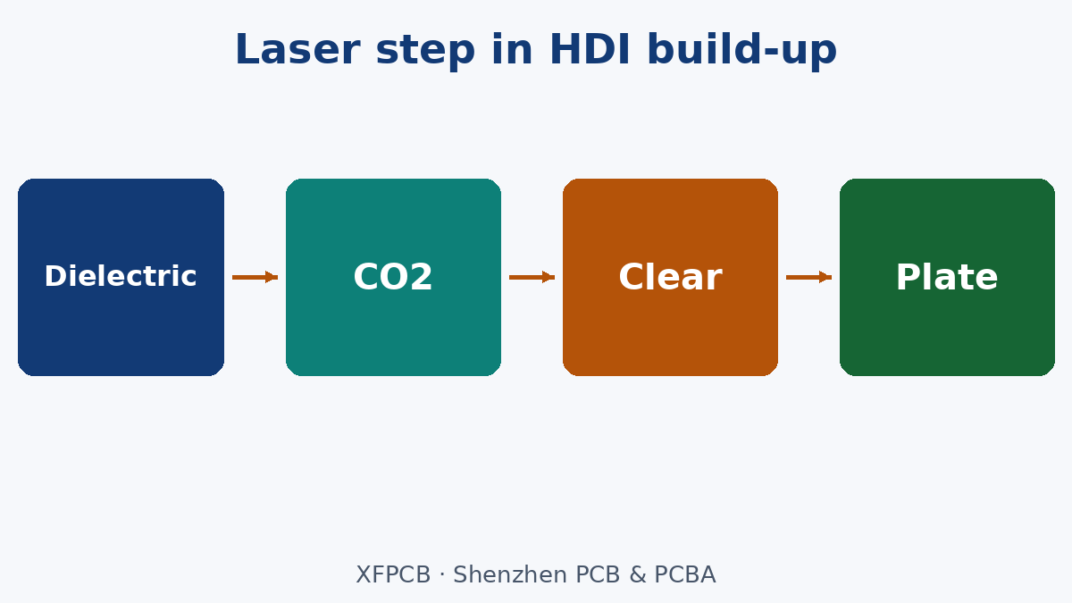
Through-holes and large vias stay mechanical in most cost models. A spindle is still the right tool for finished hole sizes in the ordinary PTH range. Hybrid panels—laser microvias plus mechanical PTH—are normal, not a compromise.
Mechanical versus CO₂—decision, not slogan
| Need | Usual tool |
|---|---|
| Blind microvia in dielectric to a copper pad | CO₂ laser (often) |
| Very fine copper+dielectric machining | UV laser family |
| Through-hole / larger finished hole | Mechanical drill |
| Flex coverlay opening | Flex laser process (separate) |
Do not put “laser drill all holes” on a drawing that still needs press-fit PTH barrels. Do not put a mechanical micro-bit callout on a 1+N+1 build-up that was quoted as laser microvia.
What the factory needs on the note
- Which layers are microvia (start–stop layer pairs).
- Capture pad presence and any copper-open recipe before CO₂.
- Target finished via architecture (filled/capped if required for stacked vias)—as a callout, not a hope.
- Which holes remain mechanical PTH.
- Inspection expectation for via fill or plating if that is a product requirement (microsection program, not e-test alone).
Our HDI PCB Capability page is the capability conversation; the drawing still has to name the stop layers.
What we are not claiming
No universal micrometre floor, no claim that CO₂ replaces UV, no claim that laser removes tool cost from every panel, and no flex-coverlay procedure disguised as HDI. CO₂ laser HDI drilling is dielectric ablation to a copper stop, then clear and plate. Leave PTH to the bit unless the quote explicitly says otherwise.