
Printed electronics and conventional PCB fab solve different problems with different materials. Conductive ink lays down a printable conductor on film, paper, textile, or rigid laminate. Etched copper on FR-4 or polyimide still carries most product power, RF, and dense digital nets. Buyers who treat "conductive ink" as a drop-in replacement for copper, or who confuse printed traces with electrically conductive adhesive (ECA) attach, end up with RFQs that no fab can quote apples-to-apples.
This factory buyer guide defines conductive ink printed electronics against etched PCB practice, walks ink families (silver, copper, carbon/graphene, polymer) by resistivity, cost, oxidation, and flex behavior, shows where printing wins versus where China rigid and flex PCB fab still wins, covers hybrid builds that combine both, and lists RFQ fields that keep quotes comparable. It does not invent a specialty print line you did not ask for. Confirm sheet resistance, cure, substrate, and bend life on your drawing and PO; market slogans are not acceptance criteria.
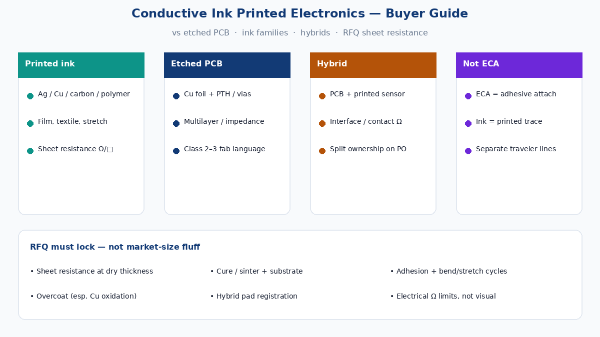
Printed conductor vs etched copper — different stacks, different jobs
Conductive ink printed electronics deposits a filled ink or paste (metal, carbon, or conductive polymer) onto a substrate by screen, stencil, inkjet, gravure, or similar methods, then cures or sinters so the print conducts. Typical substrates include PET, PI film, paper, textiles, glass, and sometimes rigid laminate. Line width, thickness, and sheet resistance are set by print process and ink, not by copper foil weight and etch undercut.
Conventional etched PCB starts with copper foil laminated to rigid FR-4, polyimide flex, or metal-core stock. Photolithography and etch (or additive plating) form nets; plated through-holes and vias connect layers. Impedance, current capacity, and multilayer density follow IPC-familiar stackup rules that China fab lines already run at volume.
| Dimension | Printed conductive ink | Etched copper PCB |
|---|---|---|
| Conductor | Particle/polymer network after cure/sinter | Continuous metal foil / plated copper |
| Typical resistivity | Higher than bulk copper; ink- and thickness-dependent | Near bulk copper for standard foil |
| Layering | Often 1–few printed layers; vias limited or process-specific | Multilayer with PTH/blind/buried vias |
| Best fit | Large-area sensors, RFID antennas, membrane keys, stretchables, solar paste | Dense digital, power, RF, connectors, Class-controlled fab |
| Change cost | Artwork + screen/print recipe; often fast for simple 1-layer | CAM + tooling + multilayer stack; ECO cost rises with layers |
Buyer rule: if the product needs via stacks, controlled impedance, fine-pitch SMT, and documented Class 2/3 acceptance, start from etched PCB language. If the product needs ultra-thin, large-area, or stretchable interconnect with moderate conductivity, start from printed-ink language — then decide whether a hybrid is smarter than an all-print design.
Do not conflate printed conductive ink with ECA. ECA is an adhesive attach method (isotropic or anisotropic glue joints that replace or supplement solder on pads). Conductive ink is a printed interconnect or sensor layer. Both may use silver fillers; process ownership, RFQ fields, and failure modes differ. Keep them as separate traveler families.
Ink families — resistivity, cost, oxidation, flex tradeoffs
Commercial inks are engineered systems (filler + binder + solvent/rheology), not "paint with metal." Families buyers meet most often:
Silver (Ag) flake / nanoparticle inks and pastes
Lowest practical resistivity among common printable metals when cured or sintered correctly. Higher material cost. Oxidation is milder than copper at room conditions, which is why Ag dominates many membrane switches, RFID antennas, and medical sensor prints. Nanoparticle systems can sinter at lower temperatures — useful on PET — but price and process windows are tighter. Watch adhesion to film, silver migration under humidity/bias, and bend crack if the binder is brittle.
Copper (Cu) inks and pastes
Attractive on raw metal cost. Oxidation before and after print is the factory problem: oxide skins raise resistance and kill solderability or contact quality. Many Cu systems need reducing atmospheres, flash sintering, protective overcoat, or rapid process control that not every print house owns. Use copper when cost and conductivity justify the oxidation process budget; do not assume "copper ink = etched copper reliability" without environmental and bend data on the actual stack.
Carbon / graphene / nanotube-filled inks
Higher sheet resistance than Ag or well-sintered Cu — often fine for heaters, ESD paths, resistor prints, some sensors, and low-current interconnect. Cost is usually lower than Ag for similar print area. Flex and abrasion behavior depends on binder more than on the carbon brand story. Graphene and CNT marketing claims need datasheet sheet-resistance and bend-cycle numbers, not brochure adjectives.
Conductive polymers (e.g. PEDOT-type and related systems)
Useful where transparency, stretch, or specialty sensing matters more than low ohms. Resistivity is typically much higher than metal-filled inks. Stability under humidity, UV, and wash cycles must be proven for wearables. Treat polymer conductors as a design family with their own cure and encapsulation rules.
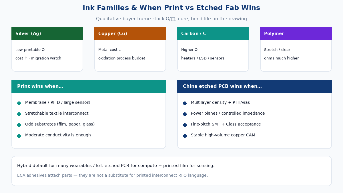
Rough buyer frame (order-of-magnitude thinking, not a quote table): Ag when you need the lowest printable ohms and can pay for it; Cu when cost pressure is high and oxidation control is funded; carbon when moderate conductivity and cost win; polymer when stretch/transparency dominate. Always lock sheet resistance (Ω/□) at specified dry thickness, not "conductive ink, silver type" alone.
Where printed electronics wins
Printing earns its keep when geometry, substrate, or cost structure beat etched copper:
- Membrane switches and simple HMI overlays — large areas, few layers, tactile stacks on PET; Ag or carbon traces are industry-standard.
- RFID / NFC antennas and smart packaging — high unit counts, thin film, cost per antenna dominates; print + wet/dry inlay beat multilayer PCB for many tags.
- Large-area sensors — pressure, humidity, temperature, or biomedical patches on film where a full PCB would be overkill.
- Stretchable / textile wearables — elastomeric or fabric substrates that etched FR-4 cannot follow; stretchable Ag or polymer systems (with encapsulation) when the product is clothing-like, not a rigid compute brick.
- Solar cell metallization pastes — high-volume paste print on cells; a different industry line than PCB fab, but the same buyer lesson: paste spec and fire/cure window own yield.
- Rapid one-layer interconnect on odd substrates — glass, paper, molded plastic — where laminating copper foil is impractical.
In these cases the "PCB" may be a printed film that never sees a drill or plating line. Quoting that work on a multilayer rigid RFQ form produces noise.
When China rigid / flex PCB fab still wins
China etched PCB capacity wins when the product looks like a board buyers already know how to buy:
- Multilayer density — BGA escapes, buried capacitance needs, many nets per cm².
- Current and thermal — power planes, heavy copper, metal-core, thermal vias.
- RF / controlled impedance — stackup Dk/Df control, reference planes, tight etch tolerance.
- Fine-pitch SMT and connectors — ENIG/OSP finishes, solder mask dams, ZIF tails, stiffeners on flex.
- Documented reliability classes — IPC Class 2/3 visual and acceptance language, Coupons, microsections, flying-probe/bed-of-nails e-test on copper nets.
- Volume with stable CAM — once Gerbers freeze, panelization and plating economics beat custom print screens for complex interconnect.
A stretchable shirt sensor is a print problem. A four-layer drone flight controller or an industrial HMI motherboard is a PCB fab problem. Forcing either into the wrong process family burns NRE and schedule.
Flex PCB (etched copper on PI with coverlay) is not the same as printed stretchable ink on TPU. Both bend; copper flex follows IPC flex design rules and plated vias, while stretchable print follows ink elongation and wash/encapsulation specs. Call the family on the RFQ.
Hybrid builds — PCB plus printed traces or sensors
Many real products are hybrids, not either/or:
- Rigid or flex PCB carries MCU, power, RF, and connectors in etched copper.
- Printed sensor, antenna, or heater lives on film or on a selective print region, then connects by ACF/ACA, ZIF, conductive PSA, crimp, or soldered tails where metallurgy allows.
- Selective print on PCB — some lines print carbon resistors, heaters, or shielding patterns onto finished laminate as an additive step. That is still a print process add-on, not a claim that every fab runs inkjet copper for all nets.
Hybrid RFQ discipline:
- Separate drawings or clearly layered CAD for the etched board vs the printed part.
- Interface definition: connector P/N, ACF type, contact resistance limits, peel/adhesion tests.
- Environmental ownership: humidity, sweat, wash, flex cycles on the printed side; vibration and Class acceptance on the PCB side.
- Do not ask a copper fab to "just print the antenna" without naming ink family, sheet resistance, cure, and who owns registration to copper pads.
Industry practice includes hybrids; that is not the same as claiming any one plant prints every conductive-ink geometry in-house. Source print and fab from qualified partners when needed, and keep the interface on the PO.
RFQ and spec fields that make quotes comparable
Market fluff quotes "$2B ink markets" and lists filler classes. Factories quote from fields. Put these on the RFQ or drawing notes:
| Field | Why it matters |
|---|---|
| Sheet resistance (Ω/□) at target dry thickness | Conductivity without thickness is meaningless |
| Ink family / qualified P/N list | Ag vs Cu vs carbon vs polymer change process and cost |
| Print method | Screen, stencil, inkjet — resolution and thickness differ |
| Cure / sinter profile | Time–temperature (or photonic sinter) ownership |
| Substrate | PET, PI, TPU, textile, glass, FR-4 — Tg and adhesion differ |
| Adhesion test | Cross-hatch, peel, or tape method + accept limit |
| Bend / stretch cycles | Radius, elongation %, cycle count, resistance drift limit |
| Environmental | 85/85, salt, wash, sweat, UV as applicable |
| Overcoat / encapsulation | Required for Cu oxidation and wearable wash |
| Registration to copper / mechanics | Hybrid pad alignment tolerances |
| Electrical test | Continuity, Ω limits, not "visual OK" |
| Lot / shelf-life rules | Ink pot life and substrate moisture |
If the RFQ only says "conductive silver ink for wearables," expect either a no-quote or a sample that fails your bend and wash test. Mirror the discipline you already use for copper weight, impedance, and surface finish on etched boards.
Process notes buyers forget (and fabs price later)
Print yield is not free once artwork looks simple. Screen mesh, emulsion thickness, and ink rheology set wet deposit; under-deposit raises ohms, over-deposit bridges fine gaps and wastes Ag. Inkjet needs different viscosity and nozzle maintenance than screen paste. Photonic or oven sinter windows that work on PET may scorch TPU or leave Cu under-reduced.
On hybrids, registration between printed antenna edges and copper pads drives scrap as often as raw resistivity. Ask who owns first-article: print house, PCB fab, or system integrator. Put contact resistance after assembly (not only printed sheet resistance) on the acceptance sheet when the print mates to a board.
Carbon prints used as resistors need tolerance language (±%) and trim method if any. Treating a carbon meander as "about 1 kΩ" without a measurement plan is how membrane lots drift out of feel and LED drive current.
Soft next step for buyers
Start with the job, not the buzzword. If the interconnect must look like a multilayer PCB, write a China rigid/flex fab RFQ with stackup, copper, finish, and test coverage. If the interconnect must live on film, textile, or stretchable skin, write a printed-electronics RFQ with sheet resistance, cure, substrate, and bend life — and decide early whether a hybrid PCB + print module is cheaper than forcing one process to do both.
When you are ready to compare options, share the substrate, target ohms, bend or stretch duty, and whether power/RF still need conventional copper. A clear split between etched fab scope and print scope beats another round of market-size slides.