
Searchers who type flip board PCB usually mean one of two things: flip-chip packaging and board attach (die or FC-BGA on a PCB), or an EDA “flip board / mirror board” CAD operation. This playbook is the first meaning — factory DFM and RFQ language for flip-chip attach and finished FC-BGA at board level. EDA mirror/flip is called out once so quotes and drawings stay in the packaging lane. It is not a BGA/CSP package catalog and not an HDI flex micro-bump process tour; those stay at their own boundaries.
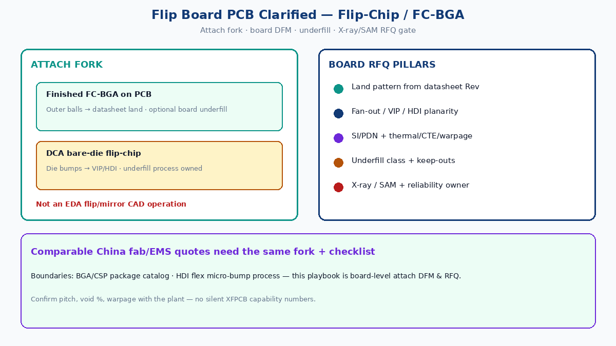
Quick answer: name the attach, then RFQ the board + EMS gate
- Disambiguate the search intent — packaging flip-chip / FC-BGA on a PCB, not an EDA “flip board” mirror. Put the CAD operation in a one-line drawing note; keep the fab/EMS RFQ in packaging language.
- Separate attach method from package form — flip-chip is how the die faces the carrier (bumps down). FC-BGA is a finished package that already used flip-chip inside and presents BGA balls to your board. Direct chip attach (DCA) bare die on PCB is a different RFQ from soldering a finished FC-BGA.
- Lock board-level DFM before paste — land pattern from the package datasheet (not a guessed pad), fan-out / via-in-pad / HDI rules, SI and PDN under the die shadow, thermal and CTE stack, and surface finish compatible with the bump/ball alloy.
- Specify underfill + inspection + reliability — underfill class and process window, X-ray (and SAM when voids or delam risk matter), void/bridge criteria, and thermal-cycle / drop / moisture language buyers must put in the RFQ — not hope the EMS “does BGA like usual.”
- Issue a China fab/EMS comparable checklist — same attach type, same land/via rules, same underfill and inspection clauses on every quote so plants cannot silently swap DCA for FC-BGA or skip underfill.
Factory tip: “Flip board” in a buyer email is ambiguous. Reply with: attach type (DCA bare die vs finished FC-BGA), land pattern source (datasheet revision), underfill yes/no + class, X-ray/SAM plan. Until those four are locked, stencil, HDI, and reliability quotes are not comparable.
What “flip board” is not (EDA mirror — short)
In many EDA tools, flip board or mirror board means reflecting the PCB design about an axis for panelization, dual-sided artwork, or mechanical fit. That is a CAD operation. It does not define bump pitch, underfill, or FC-BGA land patterns. If your supplier asks “do you need flip board?” and means packaging, answer in attach language. If your layout team means CAD mirror, keep that request out of the fab process notes so CAM does not invent a packaging step.
Flip-chip attach ≠ BGA package form
| Term | What it is | What your board RFQ must name | Common mix-up |
|---|---|---|---|
| Flip-chip (attach method) | Die face-down; bumps/pads join to carrier lands | Carrier type (package substrate vs PCB), bump/land pitch class, underfill | Calling any BGA “flip-chip” |
| FC-BGA (finished package) | Flip-chip die already attached inside a BGA package; outer balls solder to your PCB | Package P/N, ball map, datasheet land pattern, reflow + underfill (if required at board level) | Treating outer balls as die bumps |
| DCA / bare-die flip-chip on PCB | Bare die bumped and attached directly to the PCB (or interposer on PCB) | Die bump map, PCB land + VIP/HDI, underfill process owned by EMS/OSAT path | Quoting like a standard BGA SMT job |
| Wire-bond BGA / other BGA | Different first-level interconnect inside the package | Still a BGA land pattern — but not flip-chip language | Using flip-chip underfill notes blindly |
Rule for buyers: flip-chip describes orientation and first-level join. BGA / FC-BGA describes what lands on your second-level board. A finished FC-BGA may need board-level underfill for reliability; a DCA bare-die job always needs a bump-land-underfill process definition. Do not paste one RFQ paragraph onto the other.
Boundary note: package family selection and CSP/BGA form-factor tradeoffs belong in a BGA/CSP packages guide. Raised interconnect on thin HDI flex belongs in a flex micro-bump array playbook. This article stays on board-level DFM and assembly RFQ once you already know you are attaching flip-chip or placing FC-BGA.
DCA bare die vs finished FC-BGA — RFQ fork
Finished FC-BGA on PCB (typical PCBA path)
- You buy a packaged device; outer solder balls reflow to PCB pads.
- Land pattern, stencil, and reflow profile follow the package datasheet and the EMS’s BGA process control.
- Board underfill may still be required for drop, thermal cycle, or fine-pitch reliability — call it out; do not assume “BGA = no underfill.”
- Inspection is usually 2D/3D X-ray on ball joints; SAM is less common at board level unless underfill or delam is in scope.
DCA / bare-die flip-chip on PCB (higher process ownership)
- Die bumps attach to PCB (or a board-mounted interposer). Pitch and coplanarity are die-driven.
- PCB needs matched land geometry, often via-in-pad / HDI fan-out, controlled flatness, and a finish compatible with the bump metallurgy.
- Underfill (and sometimes capillary vs molded / wafer-applied class language) is part of the assembly process, not an optional coating.
- Yield risk sits in bump-land alignment, underfill voids, and CTE mismatch — not only in “SMT paste volume.”
If the RFQ only says “flip chip BGA, China assembly,” plants will quote different machines, different underfill materials, and different inspection depth. Force the fork in the first line of the RFQ.
Board-level DFM: fan-out, VIP/HDI, SI/PDN, thermal/CTE, land pattern
Land pattern from the datasheet — not from memory
For FC-BGA, copy the recommended land pattern, solder mask defined vs non-solder mask defined preference, and paste volume notes from the current datasheet revision. For DCA, the land map comes from the die bump drawing plus the assembly house’s process window. Changing pad diameter “a little for yield” without plant agreement moves bridges and opens in opposite directions.
Fan-out and via-in-pad / HDI
Dense ball or bump fields push escape routing into via-in-pad (VIP), microvia, and HDI stack choices. Spec:
- Whether VIP is filled and plated flat (critical under BGA/FC lands).
- Microvia stack (staggered vs stacked) and any keep-out under the die shadow.
- Copper balance and local thickness so the land field stays coplanar through reflow.
Unfilled or poorly planarized VIP under fine-pitch balls is a classic void and open driver. Ask the fab to state VIP planarity class on the quote, not only “HDI capable.”
SI and PDN under the package shadow
Flip-chip and FC-BGA often sit on high-speed or high-current silicon. Lock return-path continuity under the ball/bump field (via density with the SI owner — do not invent via counts here), decoupling the ball map actually allows, and PDN splits that do not island the die shadow. SI/PDN is design ownership; the fab owns stack-up impedance and via fabrication. Put both on the RFQ so nobody owns neither.
Thermal and CTE
Heat leaves through the ball/bump field, copper, and sometimes a lid path. Spec local copper/thermal vias per datasheet and fab drill/fill rules; laminate Tg/CTE class for reflow count and field cycle (critical for DCA where silicon meets organic PCB); and a warpage window for PCB and package at reflow. Large FC-BGA on thin boards fails when warpage and ball collapse fight each other. Do not put fabricated millimetre or ppm numbers from a blog — write “thermal via / CTE / warpage limits per datasheet + fab agreement.”
Surface finish and alloy compatibility
OSP, ENIG, and other finishes behave differently under fine-pitch BGA and under bump attach. Lock finish with the bump/ball alloy and the number of reflow cycles. Mixed finishes on the same panel under the FC field need an explicit process note.
Underfill, inspection, and reliability language buyers must RFQ
Underfill
Underfill redistributes stress away from individual bumps/balls and reduces fatigue and drop damage. RFQ must say:
- Required or not at board level (and why: pitch, drop, thermal cycle, automotive/industrial class — without inventing XFPCB cert claims).
- Process class the EMS will run (e.g. capillary underfill after reflow vs other plant-owned variants) — confirm availability; do not dictate a brand.
- Keep-outs for underfill flow (nearby tall parts, connectors, test points).
- Cure profile ownership and outgassing / cleanliness constraints if conformal coat or potting follows.
“Underfill if needed” is not a process instruction. Either require it with acceptance criteria or explicitly waive it with a reliability owner’s signature.
Inspection: X-ray and SAM language
- X-ray (2D/3D as agreed): ball/bump voids, bridges, missing joints, head-in-pillow class defects on BGA. Define sample plan (100% vs AQL) and void % criteria with the EMS — blog % figures are not acceptance defaults.
- SAM (scanning acoustic microscopy): useful when underfill voids, delamination, or die-attach integrity are reliability-critical. Not every consumer BGA job needs SAM; high-reliability and DCA programs often do. Name it when you need it so quotes include equipment time.
- Optical / AOI: limited under the package body; do not treat top-side AOI as a substitute for joint inspection.
Reliability concerns to put in the RFQ (not after NPI failure)
Ask every plant the same set: reflow profile ownership and max cycles; underfill void/fillet criteria and rework policy (many underfilled parts are not rework-friendly); thermal-cycle / drop / humidity test ownership and standard class (confirm — do not invent a standard number as an XFPCB promise); MSL handling and bake-out; warpage measurement method for PCB and package at reflow temperature class.
China fab / EMS comparable RFQ checklist
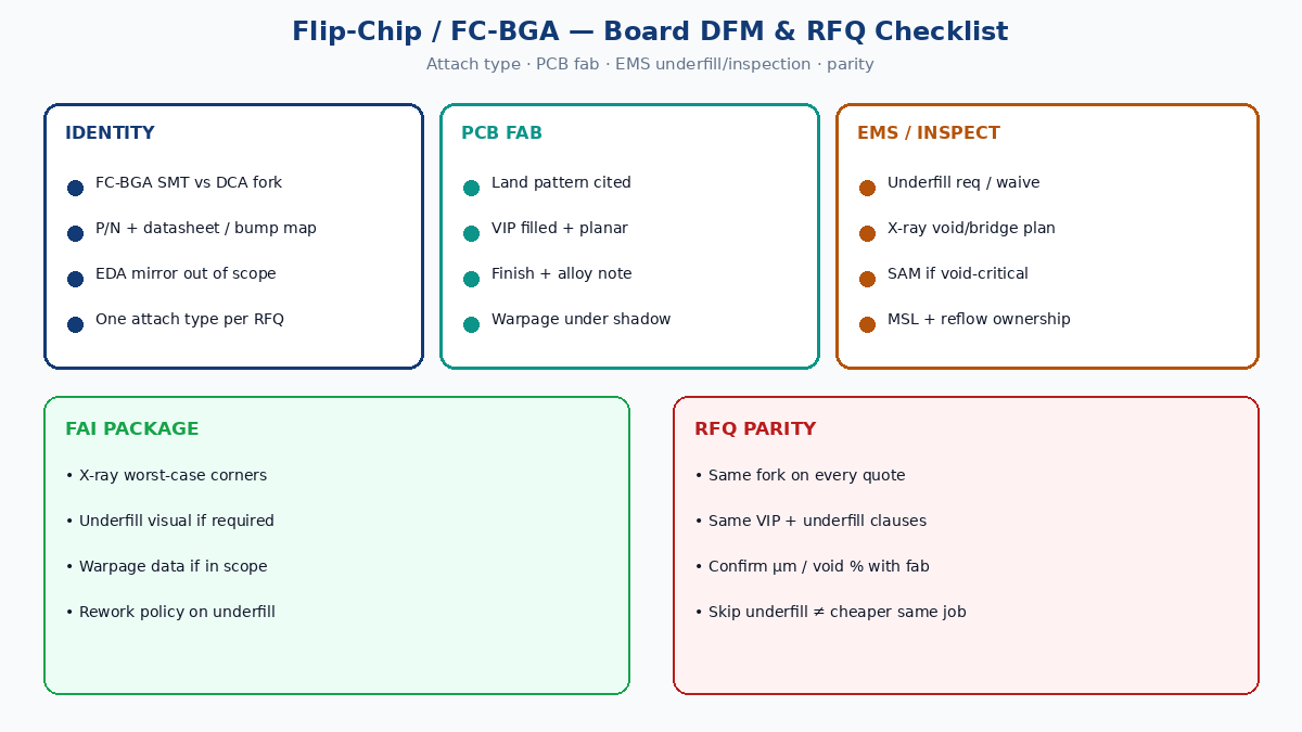
Use one checklist on every quote so “flip chip” does not mean three different process families.
Identity
- [ ] Attach type locked: finished FC-BGA SMT vs DCA bare-die flip-chip (one box only).
- [ ] Package or die P/N + datasheet / bump-map revision dated.
- [ ] EDA “flip board” CAD mirror explicitly out of scope in process notes.
PCB fabrication
- [ ] Land pattern source cited; NSMD/SMD preference stated.
- [ ] VIP / microvia / HDI stack and planarity class under the field.
- [ ] Surface finish + alloy compatibility note.
- [ ] Warpage / flatness expectation under the package shadow.
- [ ] Impedance / stack-up callouts if SI-critical nets escape the field.
Assembly / EMS
- [ ] Stencil and paste volume plan (or die-attach process class for DCA).
- [ ] Underfill: required / waived; process class; keep-outs; cure ownership.
- [ ] X-ray plan + void/bridge criteria; SAM yes/no and sample plan.
- [ ] Reflow / attach profile ownership; MSL / bake.
- [ ] Rework policy for underfilled devices.
- [ ] FAI package: X-ray images of worst-case corners, underfill visual if applicable, warpage data if required.
Comparability rule
- [ ] Same checklist answered by every plant. A cheaper quote that skips underfill or VIP planarity is a different product.
Drawing and CAM notes that prevent silent swaps
Put process-critical text on the fab/assembly drawing, not only in email: land pattern per datasheet Rev X (no silent pad swaps); VIP filled and plated flat with planarity class; underfill required/waived + keep-out; X-ray sample plan and SAM if void criteria apply; “not an EDA flip/mirror instruction.” Ambiguous “flip chip OK” becomes the plant’s default BGA recipe under time pressure.
What this playbook deliberately does not cover
- BGA vs CSP package family selection and ball-pitch catalogs — separate packages guide boundary.
- HDI flex micro-bump array process (paste vs electroplate on thin FPC) — separate flex micro-bump boundary; do not mix flex bump height FAI into an FC-BGA PCB RFQ.
- OSAT substrate design for building the FC-BGA package itself — that is package-substrate work, not commodity PCB RFQ language.
- Competitor brand process tours — specify process classes and acceptance criteria; confirm capability with the plant you actually buy from.
Closing: RFQ gate in one paragraph
When someone asks for a flip board PCB, answer with packaging clarity: flip-chip attach versus finished FC-BGA, datasheet land pattern, VIP/HDI and SI/PDN under the shadow, thermal/CTE and warpage, underfill yes/no with process class, and X-ray/SAM plus reliability ownership. Put the same checklist on every China fab and EMS quote. Confirm every pitch, void %, and warpage limit with the plant — treat industry conversation bands as starting points, never as silent XFPCB capability guarantees. That is the assembly RFQ gate; everything else is CAD vocabulary or a different article.