
A flying-lead flex PCB (also called dual-access, back-bared, or reverse-bared flex) exposes the same copper conductor from both faces in a defined window by removing coverlay on one side and base film on the opposite side. That is a selective dielectric-removal feature on a single conductor path — not a double-sided via interconnect between two copper layers. Before you freeze drawings or send a China fab RFQ, lock five decisions in this order: structure class (1S dual-access vs 2S flying-lead complexity), window both sides (size, registration, residual film), process route (pre-cut coverlay vs laser / plasma / chemical for small windows), mechanical support (lead length, width, support island), then finish + FAI. Micrometre and millimetre figures in this playbook are industry starting guidance only; confirm every µm/mm and process class with your fab.
Factory tip: Dual-access copper is thin and locally unsupported after both dielectrics are cleared. Treat the flying lead as a named feature on the fab drawing — lead length, width, window both sides, support island, finish, and FAI — not as “open coverlay both sides” on a standard 1S quote. Small windows in a roughly ~1.0 mm class often leave the pre-cut coverlay route and need laser / plasma / chemical removal; confirm the cutoff with the plant, do not treat that figure as a capability claim.
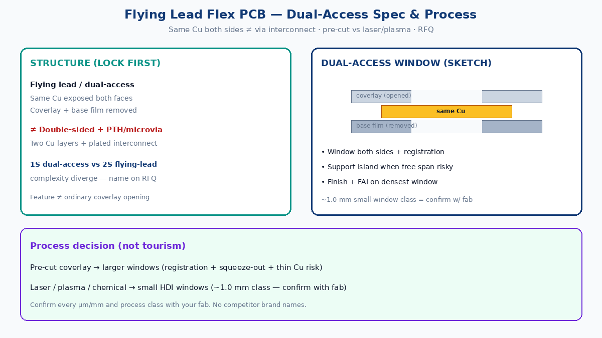
Quick answer
- Name the structure correctly — same Cu exposed both sides by coverlay + base-film removal ≠ double-sided flex with PTH/microvia interconnect. If you need two copper nets tied by vias, that is a different build family.
- Choose 1S vs 2S flying-lead complexity early — 1S dual-access is one conductor layer with selective back-bared access. 2S adds copper on both faces of the base film; flying-lead windows must declare which copper, which dielectric, and how much support remains — process risk and quote language diverge.
- Trigger the feature from the use-case — TAB / chip bonding, fine HDI contact, probe / compression pads, or other dual-face access needs. Brief use-case language on the RFQ stops plants from quoting ordinary coverlay openings.
- Pick process by window class — pre-cut coverlay works for larger windows when registration and adhesive squeeze-out stay inside tolerance; for small windows (buyers often discuss a ~1.0 mm class and below — confirm with fab), laser ablation, plasma, or chemical selective removal usually owns edge quality and copper protection.
- Issue RFQ with drawing notes + FAI — lead length/width, window both sides, support island, finish, residual film/adhesive limits, and first-article photo/measurement criteria. Ask every plant the same questions so quotes are comparable.
Structure: dual-access copper ≠ double-sided via interconnect
In a conventional single-sided flex, copper sits on base polyimide (or adhesiveless PI) and is protected on the opposite face by coverlay. One face of the conductor may be accessible through a coverlay opening; the other face remains backed by base film.
A flying-lead / dual-access zone clears both insulating layers locally:
- Coverlay (and its adhesive) is opened on one face.
- Base film is selectively removed on the opposite face at the same XY location.
- The same copper ribbon or land is then free on both faces for bonding, soldering, probe contact, or other dual-face connection.
That stack is still typically a single conductor path through the window. There is no requirement for a second copper layer or for plated through holes to “connect top to bottom” — the top and bottom of the window are two faces of one foil.
| Build language | Copper layers in the window | How both faces are reached | What the fab must own |
|---|---|---|---|
| Flying lead / dual-access / back-bared | One conductor (same Cu both faces) | Selective coverlay + base-film removal | Registration of both windows, Cu protection, residual dielectric/adhesive limits |
| Double-sided flex + PTH / microvia | Two (or more) conductor layers | Plated barrel or microvia interconnect | Via design, plating, bend keep-outs — different playbook |
| Ordinary 1S coverlay opening | One conductor, one accessible face | Coverlay window only; base film remains | Coverlay cut / registration for SMT or land access |
Buyers and plants lose yield when RFQ text says “double-sided flex” but the drawing only needs dual-access on one copper. Dual-access is often cheaper than a full 2S+PTH when the only need is back-side access to selected features — and harder than a catalog 1S because base-film removal, thin unsupported Cu, and dual-window registration are specialty steps. Name the feature explicitly.
1S vs 2S flying-lead complexity
1S flying lead (classic dual-access): one copper layer. Process intent is: form the coverlay opening on the “front,” remove base film on the “back” in registration, leave defined support around the lead. Quote language should say dual-access / flying lead / back-bared — not “1S standard.”
2S flying lead: copper exists on both sides of the base film (with or without PTH elsewhere on the panel). Complexity jumps because the fab must declare:
- Which copper face(s) become flying leads.
- Which dielectric is removed at each window (coverlay vs base film vs both).
- Whether the opposite copper remains, is etched clear, or is protected as a support frame.
- How registration stacks when two copper patterns and multiple dielectric openings share one XY zone.
A 2S panel can still host a local dual-access feature on one copper without making every net a via interconnect. Do not let CAM assume “2S = PTH everywhere” or “flying lead = open both coverlays and hope.” Put a construction note on the fab drawing: layer stack at the window, removal sequence class, and keep-out from plated holes or bend hatches.
Complexity drivers (both 1S and 2S): thinner Cu tears more easily once both dielectrics leave; longer free spans raise handling risk; narrower leads aggravate squeeze-out and laser heat damage; dense arrays need FAI photos of the worst window, not one golden sample.
Use-case triggers (brief)
Use-cases are RFQ triggers, not a catalog: TAB / chip or wire bonding (clean dual-face bond finger, residual film limits); HDI fine contact where a second copper + via stack is unjustified; probe / compression / test pads after dielectric clear-out; selective solder or conductive-adhesive attach on the face assembly actually sees. Ordinary SMT coverlay openings, micro-bump arrays, and ZIF/FFC tails are different RFQ lines — do not mix them into flying-lead notes.
Process route: pre-cut coverlay vs laser / plasma / chemical
Process choice follows window size, registration budget, adhesive behavior, and copper damage risk — not brochure tourism.
Pre-cut coverlay (and companion base-film windows)
Typical route for larger dual-access zones: pre-cut coverlay openings → laminate to copper (or patterned flex) with registration → pattern/etch per the fab’s owned sequence → selectively remove opposite base film in registration so the same Cu is free both sides.
Limits that push you off pre-cut: multi-step registration (shift leaves film on Cu or over-exposes neighbors); adhesive squeeze-out into small windows under heat/pressure; thin Cu damage (wrinkle, tear, thin at edges) on unsupported spans; small-window class — buyers and plants often discuss a roughly ~1.0 mm (and finer) class where pre-cut + laminate loses edge quality. Treat ~1.0 mm as conversation guidance to confirm with the fab — not an XFPCB cutoff and not a silent drawing default.
Laser ablation, plasma, and chemical selective removal
For small HDI flying-lead windows, fabs often clear coverlay and/or base film after stack definition using:
- Laser ablation — removes dielectric while aiming to leave Cu intact; control heat-affected zone, residue, edge taper, and Cu thinning.
- Plasma — clear-out where geometry and stack fit; put residue/undercut in the acceptance note.
- Chemical — wet selective removal where chemistry and mask allow; edge definition and Cu attack must be process-owned.
Choose by window size class, stack, Cu thickness, residue limits, and the plant’s owned recipe — not by naming equipment on the RFQ. Ask which face opens first, how thin Cu is protected, and what FAI proves (opening size, residual film, Cu integrity, densest-window photo).
| Route | Fits when | Watch-outs | Spec must say |
|---|---|---|---|
| Pre-cut coverlay (+ registered base-film removal) | Larger windows; registration and squeeze-out inside shop habit | Multi-step registration; adhesive flow; thin Cu wrinkle/tear | Cut method class, registration tolerance, squeeze-out / residual adhesive limit |
| Laser / plasma / chemical | Small windows (~1.0 mm class and finer — confirm); HDI flying leads | Heat/residue/undercut; Cu damage; process ownership | Removal process class, residual film limit, Cu damage criteria, measurement method |
Hybrid flows exist (pre-cut large zones + laser for fine fingers). If you need a hybrid, name both classes on the drawing by zone.
Design notes: lead geometry, window both sides, support island
Put geometry on the fab drawing as acceptance language, then confirm numbers with the plant:
- Lead length — free span after both dielectrics clear. Longer spans ease some bonding access and raise handling/deformation risk. State max free length or use a support island.
- Lead width — narrow leads raise registration and squeeze-out sensitivity; very narrow free Cu tears more easily. Confirm min width and Cu weight with fab for the chosen process.
- Window both sides — finished clear opening on coverlay face and base-film face; registration between them; min dielectric remaining between adjacent windows.
- Support island — intentional dielectric or Cu frame left so the lead is not a fully free flap when the duty does not need it. Mark islands on the drawing; do not leave “support TBD.”
- Bend and handling keep-outs — keep flying-lead arrays out of dynamic bend hatches and away from stiffener edges that act as stress risers into thin free Cu.
- Finish — ENIG, soft gold, OSP, or other — chosen for bond/solder/probe duty on both accessible faces if both will see the process. State whether finish is applied before or after final dielectric clear-out when sequence matters.
- FAI — photo of densest / smallest window both sides; opening size; residual film/adhesive; Cu integrity (no tear, no excessive thin); registration evidence. Netlist continuity alone does not prove dual-access quality.
Industry starting guidance (confirm with fab): small-window talks often use a ~1.0 mm class as the point where pre-cut becomes risky and laser/plasma/chemical is preferred. Lead length/width and Cu weight for free-span stiffness are plant-specific — put targets on the drawing and demand a written process class, not verbal “we can do flying lead.”
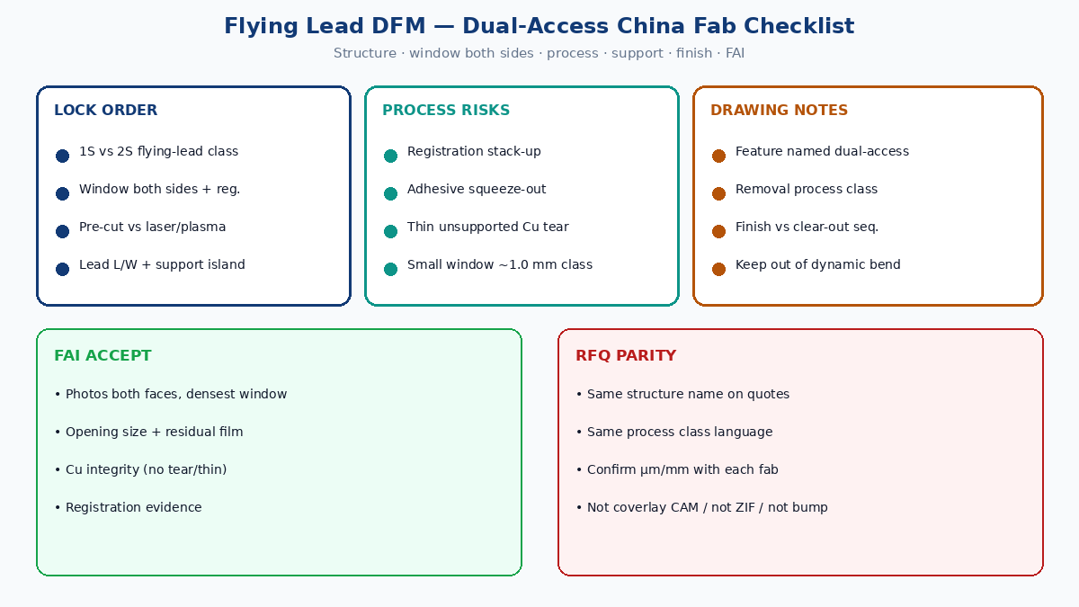
Fab drawing and China RFQ checklist
Use the same checklist for every plant so quotes are comparable:
- Structure name — flying lead / dual-access / back-bared; 1S or 2S; explicitly not “2S PTH interconnect” unless vias are required elsewhere.
- Stack at the window — Cu weight; coverlay type/thickness/adhesive class; base film type/thickness; which layers are removed on which face.
- Window both sides — finished size, registration tolerance, residual film/adhesive acceptance, min spacing between windows.
- Process route — pre-cut vs laser / plasma / chemical (or hybrid by zone); ask the plant which they will run for your window class.
- Lead geometry — length, width, count/array map; support island yes/no and dimensions.
- Finish — type, thickness class if required, and which faces receive it relative to clear-out sequence.
- FAI package — photos both faces of critical windows; dimensional checks; Cu damage criteria; sample size.
- Confirm-with-fab callouts — every µm/mm figure (including ~1.0 mm small-window class language) marked as guidance to confirm, not as a silent capability guarantee.
RFQ parity questions to ask every fab:
- For our window size class, do you run pre-cut coverlay or laser/plasma/chemical clear-out?
- What registration and residual adhesive/film limits will you accept on FAI?
- What min lead width / max free length / Cu weight do you recommend for unsupported dual-access?
- How do you protect thin Cu during base-film removal and handling?
- Will finish be applied so both cleared faces meet the bond/solder/probe duty?
What this playbook is not
This article is the dual-access / flying-lead feature: structure distinction from via interconnect, 1S vs 2S complexity, brief use-case triggers, process route for windows, and design/RFQ/FAI. It is not coverlay opening accuracy CAM for ordinary SMT pads, not a flexible-PCB types naming map (flying lead is only named there as a special), not micro-bump array selection, and not ZIF/FFC connector-tail DFM. Keep those RFQ notes on their own lines so plants do not mix process families.
Close
Lock structure and use-case first, then window-both-sides geometry, then process by window class (~1.0 mm small-window language = confirm-with-fab guidance), then support, finish, and FAI. A clean dual-access quote names the feature, removal process class, and acceptance criteria so first articles prove the same Cu is clear on both faces without tears, residual film, or registration surprises.