
Flying probe testing (FPT) is the fixtureless electrical gate most China fab and EMS houses use when a bed-of-nails ICT fixture is not yet justified. Robotic probes land on pads, vias, and component leads from CAD-driven coordinates and measure opens, shorts, resistance, capacitance, and polarity — without a custom nail plate. It wins on prototypes, NPI, high-mix low-volume, and frequent respin work. It does not replace AOI, X-ray, first-article inspection, or a customer power-on functional test (FCT). This playbook is the method-selection, DFT, and RFQ side: when FPT beats ICT on setup cost and schedule, what bare-board vs PCBA FPT actually proves, how to leave probe access for China programming, and how to write an RFQ so quotes stay comparable. It is not a short-circuit rework workflow, not a lot-hold FAI checklist, and not a rewrite of the existing flying-probe service page.
Quick answer: when FPT wins the electrical gate
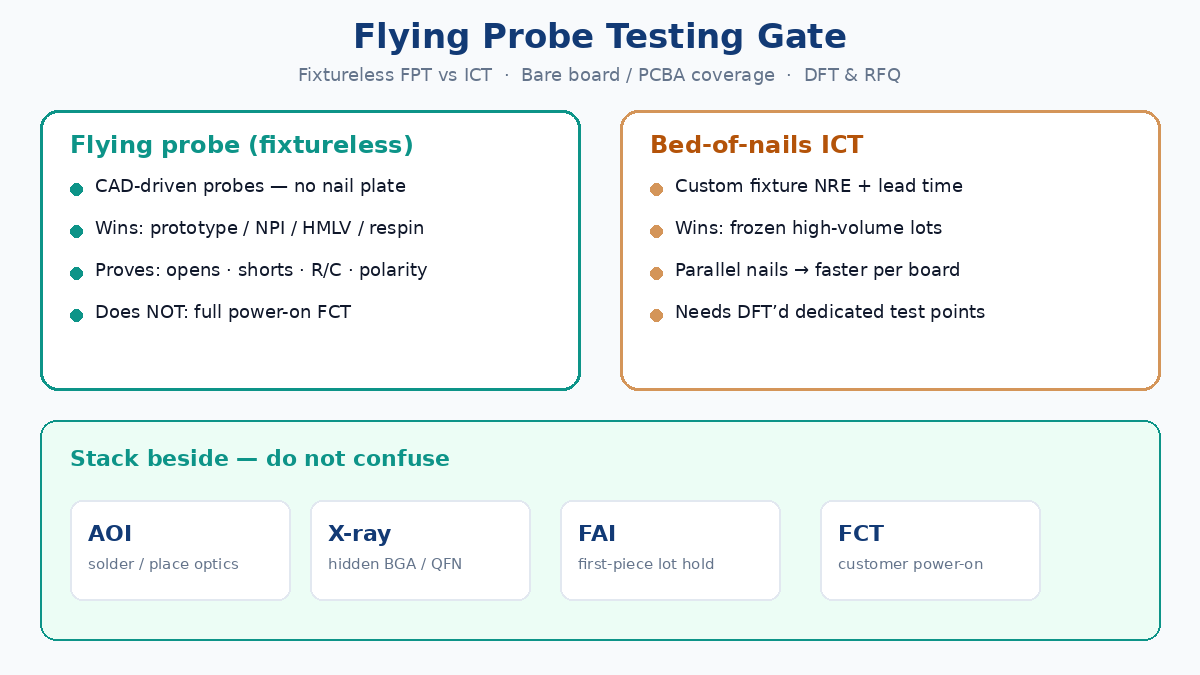
Choose flying probe when fixture NRE and wait time dominate — typically prototypes, EVT/DVT builds, pilot lots, and any SKU that will change layout before volume. Choose bed-of-nails ICT when unit count is high enough that fixture amortization and parallel nail contact beat sequential probe travel. Keep AOI for solder and placement optics, X-ray for hidden joints (BGA, QFN, bottom-terminated), and customer FCT for power-on behavior. FPT answers electrical connectivity and passive value/polarity questions; it does not certify that the assembled product boots, talks on the bus, or meets RF/power specs under load.
| Situation | Prefer FPT | Prefer ICT fixture | Still need other gates |
|---|---|---|---|
| Prototype / NPI / respin | Yes — program from CAD in hours–days | Usually no — fixture lag | AOI; FCT if functional risk |
| Low / mid volume, stable layout | Often yes until fixture ROI clears | When cycle time matters | AOI; sample X-ray |
| High volume, frozen design | Usually no — too slow per board | Yes — parallel nails | AOI + FCT line |
| Dense / fine-pitch access | Yes if pads/vias reachable | Only if nails fit the pitch | X-ray under BGA |
| Bare board electrical | Yes (opens/shorts/netlist) | Dedicated bare-board fixtures exist | Impedance coupons separate |
Fixtureless FPT vs bed-of-nails: the volume and setup gate
A flying probe machine moves a small number of probes (commonly four to eight) on gantries. Each contact is programmed; nets are exercised sequentially. A bed-of-nails ICT fixture presses hundreds of spring pins onto designated points in one stroke and can measure many nets in parallel. That difference drives the economic gate:
- Setup. FPT needs CAD/netlist programming and alignment — no nail plate. ICT needs fixture design, drill plate, wiring, and debug. When the layout is still moving, the fixture is scrap or expensive rework; FPT reprograms.
- Unit time. FPT pays probe travel for every board. ICT pays fixture NRE once, then runs faster per unit. Somewhere on the volume curve the fixture wins; the crossover is plant- and panel-specific — ask for time-per-board and fixture lead time in the RFQ rather than assuming a universal piece count.
- Access density. Fine pads and irregular geometries often favor FPT probe tips when nail diameter and fixture wiring cannot land cleanly. Conversely, a well-DFT’d high-volume board with dedicated test points is where ICT shines.
- Cosmetic mark. Probes can leave light marks on pad finish. If cosmetic class or gold-finger appearance is critical, call out allowed probe zones and accept/reject criteria up front.
Do not treat “flying probe available” as a free substitute for ICT on a frozen high-volume program. Name the method, the coverage target, and when you will re-evaluate fixture ROI after layout freeze.
Bare board vs PCBA: what FPT proves — and what it does not
Bare-board FPT (or bare-board electrical test generally) checks the fabricated interconnect against the netlist: opens, shorts, and isolation between nets. It answers whether the copper, vias, and finishes connect as designed before components land. It does not prove solderability under your process, stackup impedance (use coupons/TDR as specified), or that the assembly will function.
Assembled-board (PCBA) FPT extends probing to component terminals and test pads after SMT/THT. Typical coverage includes:
- Opens and shorts on accessible nets
- Passive value checks (R, C — and L where the platform supports it)
- Diode / LED polarity and basic semiconductor junction checks
- Orientation / polarity clues when the program and access allow
What PCBA FPT typically does not prove:
- Full power-on functional behavior (boot, firmware, protocol, RF, calibrated sensors)
- Hidden joint quality under BGA/QFN without optical or X-ray methods
- Process setup correctness for the lot (that is the FAI / first-piece gate: same stencil, feeders, programs, reflow — separate from FPT method selection)
- Root-cause repair of a hard VCC–GND short on a failed debug board (diagnosis and scrap-vs-repair workflow belongs on the short-circuit diagnostic path, not here)
Write the PO language to match the stage: “100% bare-board electrical (flying probe or equivalent)” versus “PCBA flying probe: opens/shorts + named passive/polarity list” versus “customer FCT procedure Rev X after FPT.” Mixing those phrases in one line creates quote gaps.
DFT for flying probe — guidance to confirm with the fab
Flying probe does not need a nail fixture, but it still needs landable copper. Treat the numbers below as industry starting guidance for RFQ conversation — confirm pad size, spacing, and machine class with your fab/EMS. Do not paste them into a capability claim as if every plant guarantees the same tip and force.
Practical DFT habits that raise coverage:
- Accessible pads. Prefer dedicated test pads or exposed via pads on nets you care about. Round copper with a clear solder-mask opening is easier than probing a tiny lead shoulder. Industry tables often cite pads on the order of ≥0.5 mm diameter (or comparable land) for reliable contact — confirm with the plant for your finish and probe type.
- Spacing. Leave room between probe targets so adjacent tips or successive moves do not collide with tall parts. Guidance in the ballpark of ≥0.75–1.0 mm center-to-center appears in many fab DFT notes; again, confirm.
- Mask openings. Do not bury the intended probe land under solder mask. Call out keep-outs where probing is forbidden (gold fingers, RF matching pads, soft finishes you refuse to mark).
- Fiducials. Global (and local, if dense) fiducials stabilize camera alignment so programmed coordinates match the panel. Missing fiducials raise false fails and probe misses.
- Breakouts under BGA / bottom-terminated parts. Nets trapped under a BGA ball field are invisible to a top-side probe. Fan out to probeable vias or pads outside the shadow, or accept that those nets are coverage exceptions unless you add access or use other methods.
- Height and shadowing. Tall connectors, shields, and heatsinks block probe paths. Keep clearance around critical pads or place alternate access on the opposite side if the machine supports dual-side or flip programs.
- Polarized parts. Mark clear polarity in CAD and BOM so the PCBA program can check diodes, tantalums, and LEDs instead of guessing from silkscreen alone.
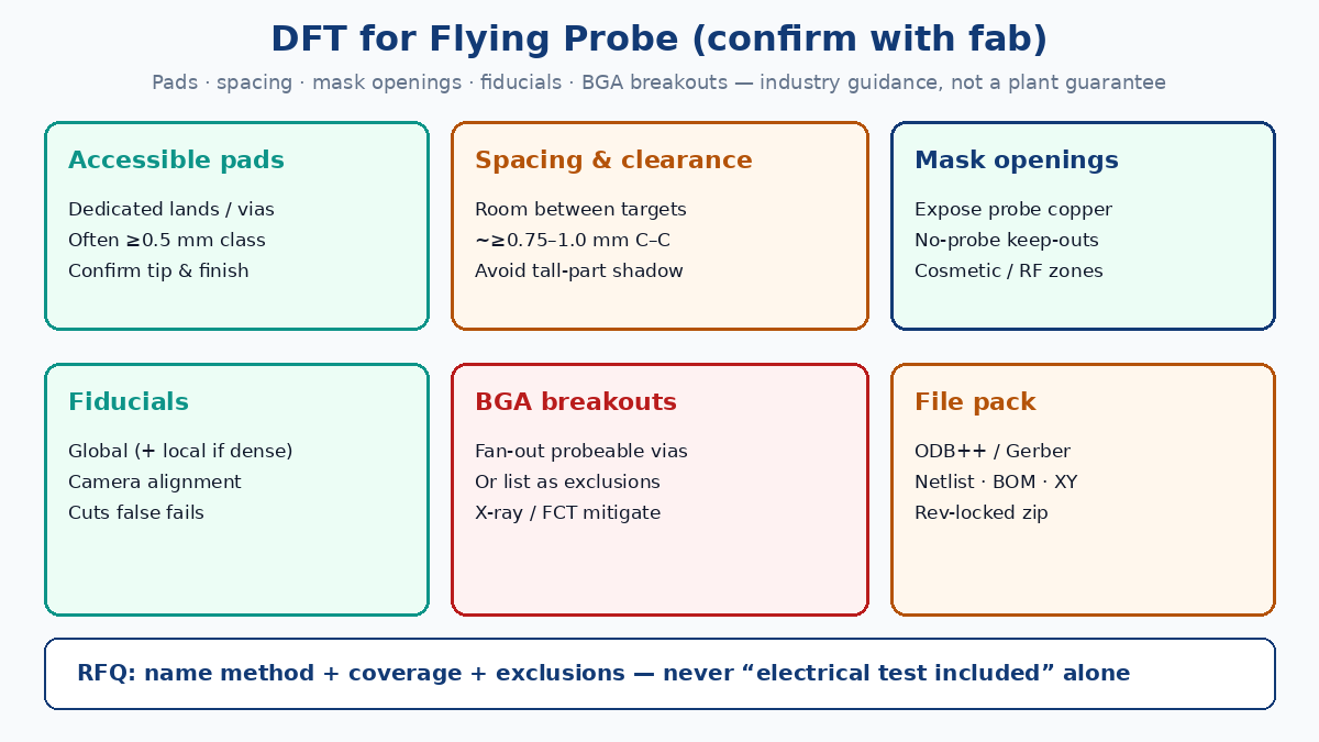
If a net cannot be probed, document it as an exclusion with the mitigation (X-ray sample, boundary scan, FCT step) rather than silently assuming 100% node coverage.
File pack the programmer actually needs
Incomplete data is the most common cause of late FPT starts and false coverage claims. Package one revision-locked zip:
- CAD / manufacturing data — ODB++ or IPC-2581 preferred; Gerbers + drill as fallback. Include solder-mask and copper layers that define probe lands.
- Netlist — IPC-D-356 or equivalent so opens/shorts map to design nets, not guessed connectivity.
- BOM — manufacturer PNs, values, tolerances, and polarity-critical flags for PCBA FPT.
- XY / centroid — pick-and-place coordinates and rotations matching the assembled revision.
- Assembly drawing / keep-out notes — no-probe zones, tall-part shadows, conformal-coat windows if coat is already applied (coated boards change access).
- Revision identity — PCB fab rev and assembly rev on the label and in the filename. A Gerber set from Rev A with a Rev B BOM is a classic false-fail generator.
Ask the house to return a short coverage note: nets probed, nets excluded, and any pads contacted on component leads instead of dedicated test points. That note belongs with the traveler, not only in a chat thread.
Stack FPT with AOI, X-ray, and customer FCT — clear boundaries
Use each tool for the defect class it sees:
- AOI — paste/solder appearance, missing/wrong polarity visible from above, tombstones, obvious bridges on exposed joints.
- X-ray — voids, hidden bridges, and open suspects under BGA/QFN and other bottom-terminated packages.
- Flying probe — electrical opens/shorts and accessible passive/polarity measurements without full product power-up.
- Customer FCT — powered exercise of the product (or a defined subset): rails, clocks, interfaces, calibration hooks.
- FAI / first-piece — production-setup release before the remaining lot; FPT may be one input to FAI evidence, but FAI is not “run flying probe and ship.”
A board can pass FPT and still fail FCT (firmware, wrong value within tolerance band the program did not check, intermittent connector). A board can fail FCT with a hard short that FPT would have caught if access and program coverage were complete — which is why DFT and the file pack matter before you argue about “test escaped.”
RFQ checklist for comparable China fab / EMS quotes
Put the same bullets in every RFQ so price and lead-time deltas mean something:
- Stage — bare board only / PCBA / both.
- Method — flying probe (fixtureless) vs ICT fixture vs “vendor choice with written rationale.”
- Coverage — 100% netlist opens/shorts; list of passives/polarity checks; explicit exclusions (e.g., nets under BGA without breakout).
- DFT assumptions — pad size/spacing class you designed to; ask the plant to confirm probe capability against that class (do not invent plant guarantees).
- Data pack — ODB++ or Gerber+netlist, BOM, XY, rev locks, keep-outs.
- Sample plan — first article only, sampling, or 100% of the lot.
- Marks and cosmeticity — allowed probe witness marks; forbidden zones.
- Sibling gates — AOI level, X-ray sample rate, whether customer FCT is in-house or buyer-supplied fixture/procedure.
- Deliverables — pass/fail report format, coverage %, fail net list, retention period.
- Respin rule — what happens to the FPT program fee when layout changes (reprogram vs waive).
Refuse vague lines like “electrical test included.” Force the method and coverage onto the quote line so two China houses are bidding the same work.
Practical takeaway
Flying probe wins when fixture NRE and layout churn hurt more than per-board probe time. Use it as the electrical connectivity and accessible-component gate on prototypes and low/mid volume; move to bed-of-nails when volume and a frozen DFT’d layout justify nails. Design probeable pads, spacing, mask openings, fiducials, and BGA breakouts — confirm sizes with the fab. Ship a complete CAD/netlist/BOM/XY pack. Stack FPT beside AOI, X-ray, FAI, and customer FCT without pretending one tool owns every defect class. Write the RFQ so every bidder prices the same coverage — that is how overseas buyers keep China electrical-test quotes honest and comparable.