
Coverlay openings on polyimide flex (FPC) decide whether SMT pads and HDI lands stay solderable after lamination. Overseas buyers RFQing China fabs usually get a materials paragraph and a cut-method claim; what actually moves yield is the CAM compensation stack — cut method tolerance, coverlay-to-pad registration, adhesive squeeze-out, and film shrinkage — then how much per-side oversize you apply relative to the stencil aperture. This playbook is factory CAM for SMT/HDI pad openings in polyimide coverlay: tolerance stack, oversize vs stencil, too-small / too-large failure modes, fab drawing notes, FAI/AOI acceptance, and RFQ questions. It is not a coverlay materials catalog and not ZIF/FFC connector-tail thickness DFM.
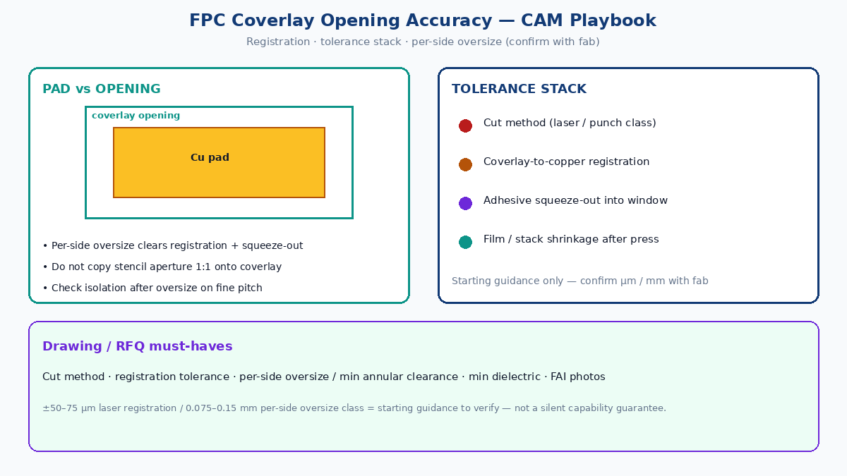
Quick answer: pad → process stack → oversize → accept
- Start from the finished pad — copper land geometry after etch, not the CAD pad alone.
- Budget a process tolerance stack — opening cut method + coverlay registration to copper + adhesive squeeze-out into the window + dimensional change after press.
- Apply per-side oversize in CAM so the as-laminated opening still clears the pad with a controlled annular margin; do not copy stencil aperture 1:1 onto coverlay.
- Watch both failure directions — too-small leaves film or adhesive on the land (skip/opens); too-large exposes adjacent copper or necks isolation on fine pitch.
- Lock numbers on the fab drawing — cut method class, registration tolerance, oversize rule, and which side(s) get openings.
- Accept on FAI/AOI with measurable criteria — opening-to-pad clearance, no film on land, isolation continuity, and first-article photos — not “looks open.”
💡 Factory gain: Put coverlay cut method, registration tolerance, per-side oversize (or min annular clearance), and FAI photo requirement on the RFQ. A quote that only says “laser coverlay” without compensation rules is not comparable across China plants.
What a coverlay opening must do for SMT / HDI
Polyimide coverlay is a pre-cut (or laser-cut) film with adhesive, laminated over copper. Every SMT pad, BGA land, and probe point that must wet solder needs an opening that:
- Fully clears the finished copper land after etch and finish.
- Leaves enough dielectric between adjacent openings so fine-pitch nets do not bridge under paste or under adhesive flash.
- Survives registration error when the film is aligned to the etched panel.
- Accounts for adhesive that flows a short distance into the window during press.
Connector wipe pads and ZIF tails have their own thickness and stiffener rules; this article stays on pad openings for SMT and HDI lands in the flex circuit body.
Process tolerance stack (the real accuracy budget)
Treat opening “accuracy” as a stack, not a single laser or punch spec:
| Contributor | What it does | Why buyers care |
|---|---|---|
| Cut method (laser / punch / plotter class) | Sets edge quality, min feature, and typical cut-to-data error | Same nominal opening size behaves differently by method |
| Coverlay-to-copper registration | Shifts the whole opening relative to the pad | Asymmetric clearance; one side of pad buried |
| Adhesive squeeze-out | Fills a ring into the opening during lamination | Shrinks the effective solderable area vs cut size |
| Film / stack shrinkage after press | Moves openings relative to copper after heat | Opens that looked centered on CAM can drift |
Industry starting guidance many fabs quote in the laser registration ±50–75 µm class and per-side oversize in the 0.075–0.15 mm class for general SMT pads. Treat those only as starting guidance buyers must confirm with their fab, stack (adhesive type/thickness), and pitch. They are not XFPCB capability guarantees and must not be copied onto a drawing as silent factory commitments.
Punch or mechanically cut coverlay often needs a more conservative oversize and larger min feature than a well-tuned laser process. Ask CAM which method applies to your panel size and opening density — do not assume the brochure default.
Per-side oversize vs stencil aperture
Stencil aperture controls paste volume. Coverlay opening controls dielectric keep-out around the land. They are related but not identical:
| Item | Typical intent | Common mistake |
|---|---|---|
| Stencil aperture | Meter paste onto the land | Copying stencil 1:1 as coverlay opening |
| Coverlay opening (CAM) | Clear finished pad + registration + squeeze-out budget | Using CAD pad = opening with zero oversize |
| Per-side oversize | Grow opening outward from pad edge on each side | Oversizing only “globally” without checking isolation |
Work the sequence:
- Lock finished pad size after etch (and any soldermask-defined vs copper-defined intent — coverlay is closer to a soldermask role on flex).
- Add per-side oversize so worst-case registration + squeeze-out still leaves bare finish on the land.
- Check remaining dielectric between adjacent openings at min pitch.
- Align stencil separately for paste volume; do not shrink coverlay to match a small stencil if that reintroduces film on copper.
On dense HDI flex, the limiting factor is often isolation between openings, not the ability to cut a larger hole. If oversize for registration would bridge two lands, you need tighter registration class, smaller adhesive flow, different pad pitch, or a process change — not a silent hope that “laser is accurate enough.”
Failure modes: too small vs too large
Too-small openings (or openings shifted onto the pad)
- Coverlay film or adhesive residue on the land → poor wetting, tombstoning risk, intermittent opens after thermal cycle.
- Partial pad exposure → paste volume low even when stencil is correct.
- AOI may pass “pad present” while SMT fails — netlist electrical test alone will not catch dielectric on copper.
Too-large openings
- Adjacent copper exposed → solder bridge risk, especially with aggressive paste.
- Trace or plane peeking at the edge of a land → impedance / leakage surprises on RF or high-impedance nodes.
- On fine pitch, overlapping effective windows after registration → hard-to-debug shorts.
Registration-dominated failure
- One side of the pad buried, opposite side over-exposed — looks like “half open” on FAI photos.
- Symmetric CAD oversize does not save you if registration eats the entire annular margin on one axis.
Plan acceptance for both directions. A shop that only screens for “opening not too small” will still ship bridge-prone panels.
Fab drawing notes that lock CAM behavior
Call these out explicitly on the fabrication drawing / notes (and mirror them in the RFQ):
| Note | Why it belongs on the drawing |
|---|---|
| Coverlay type / thickness / adhesive class | Sets squeeze-out and shrinkage behavior |
| Opening cut method class (laser vs punch, etc.) | Sets feature size and typical cut error |
| Registration tolerance coverlay-to-copper | Defines the annular margin budget |
| Per-side oversize rule or min annular clearance after lamination | Stops CAM from using pad = opening |
| Which layers / sides get openings | Avoids wrong-side coverlay windows |
| Min dielectric between adjacent openings | Protects fine-pitch isolation |
| FAI photo / AOI criteria for openings | Makes acceptance measurable |
Avoid vague notes such as “open all SMT pads” with no oversize or registration. CAM will apply a house default that may not match your stencil or pitch.
FAI / AOI acceptance (measurable, not “looks open”)
First-article and in-process checks that actually protect SMT:
- Opening fully clears the finished land on all sides within the stated min annular clearance (or documented oversize rule).
- No visible film or adhesive skin on the solderable surface at FAI magnification.
- Isolation between adjacent openings continuous — no copper peeking that should stay covered.
- Sample photos of densest pitch regions, not only sparse connectors.
- Correlate a few openings to stencil design: coverlay clear ≠ paste volume correct, but a buried pad will always starve paste.
Electrical netlist test after etch does not prove coverlay windows. Require opening-specific FAI when pitch is tight or when you are changing coverlay material, adhesive, or cut method.
RFQ questions that force comparable China fab quotes
Ask every plant the same set so quotes share one process intent:
- What coverlay cut method will you run for this panel size and opening density?
- What coverlay-to-copper registration tolerance do you commit on FAI (state as a confirmable number, not “industry standard”)?
- What per-side oversize (or min annular clearance after lamination) do you apply for SMT pads at our pitch?
- How do you account for adhesive squeeze-out in the opening size — CAM growth, process control, or both?
- What FAI photos / AOI rules do you use for openings on the densest pitch?
- If our stencil apertures are smaller than coverlay openings, will CAM still protect isolation between lands?
Attach: pad finish callout, min pitch, coverlay stack preference if any, stencil aperture summary or note that stencil is assembly-owned, and a short note that this is SMT/HDI pad openings (not connector-tail thickness).
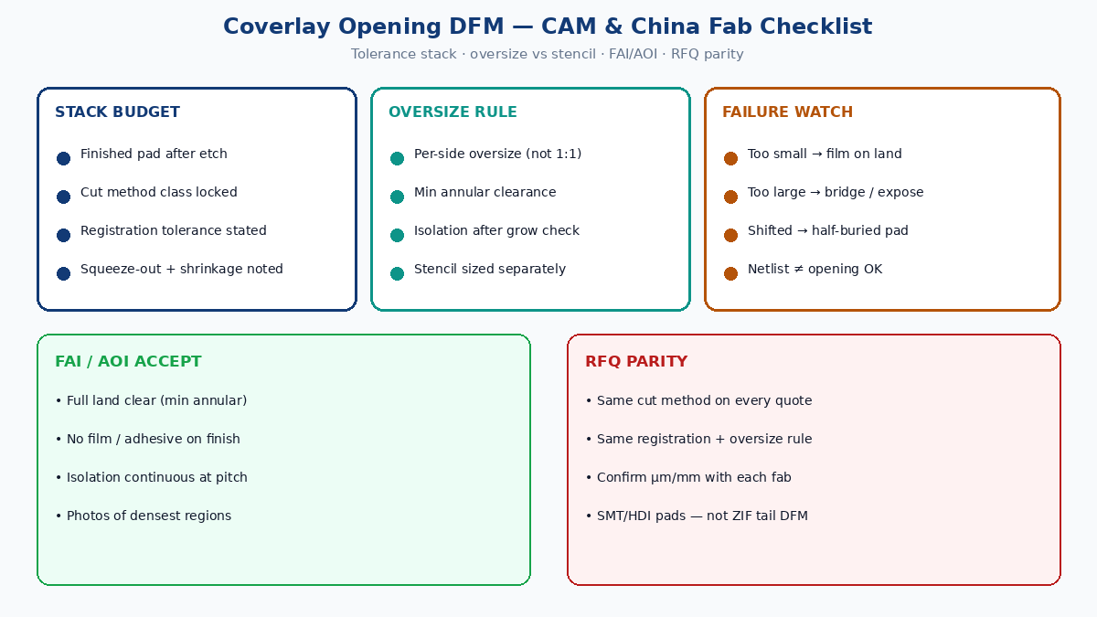
Practical CAM sequence before you lock tooling
- Freeze finished pad geometry and min pitch.
- Pick cut method class with the fab and write it on the drawing.
- Build the tolerance stack (cut + registration + squeeze-out + shrinkage) and convert it to per-side oversize or a min post-lamination clearance.
- Run a fine-pitch isolation check after oversize.
- Align stencil design separately; do not force coverlay = stencil.
- Put FAI photo requirements on the PO for densest regions.
- Only then release laser/punch tooling and coverlay artwork.
When registration or adhesive flow eats the budget, fix process class or layout — do not “add a little more oversize” until isolation fails on the next lot.
Bottom line
Coverlay opening accuracy on FPC is a CAM compensation problem: pad geometry plus cut method, registration, adhesive squeeze-out, and shrinkage, expressed as per-side oversize that still protects isolation, then verified on FAI/AOI. Materials and laser marketing lines do not replace those rules. Write the stack and acceptance into the fab drawing and RFQ so China quotes are comparable and SMT pads stay clear without bridging fine pitch.