
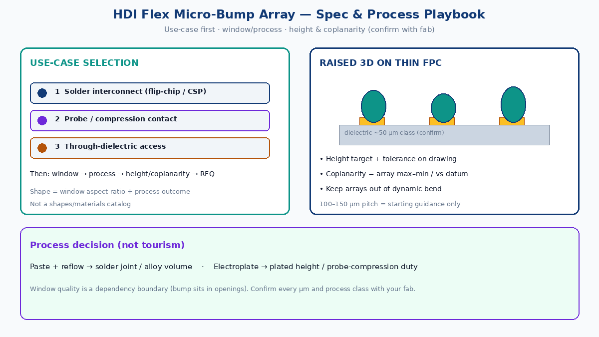
Before you release an HDI flex with a raised interconnect array, lock five decisions in this order: use-case (solder flip-chip/CSP vs probe/compression contact vs through-dielectric access), window and metal stack, process route (solder paste + reflow vs electroplate), height and coplanarity acceptance, then the RFQ and FAI package. Shape is an outcome of window aspect ratio and process — not a catalog you pick first. Pitch, bump height, and coplanarity figures in this playbook are industry starting guidance; confirm every µm and every process class with your fab before you freeze drawings.
Factory tip: On thin FPC (~50 µm dielectric class), bump height and array coplanarity fight dielectric warp and adhesive/window registration. Treat the bump as a 3D feature that lives inside a controlled opening — coverlay/mask window quality is a dependency boundary, not a second coverlay-CAM article. Keep dense bump arrays out of dynamic bend regions.
Quick answer
- Name the use-case — solder interconnect (flip-chip / CSP attach), probe or compression contact, or through-dielectric access for test/probe paths. Duty cycle and reflow exposure decide metal and process before geometry.
- Lock window location type — solder-mask/coverlay window over Cu, exposed Cu land with defined annular, flying-lead style access, or through-dielectric opening. Tie the window to the use-case; do not mix classes on one RFQ line without calling them out.
- Choose process route by criteria — paste + reflow when you need solderable volume and alloy control; electroplate when you need plated height control, finer pitch class, or a non-reflow contact duty. Decide with height tolerance, pitch, alloy, and fab capability — not by brochure tourism.
- Set height and coplanarity acceptance — define target height, tolerance band, and array coplanarity (or max–min height) on the fab drawing. On thin dielectric, confirm how the plant measures (optical, laser, or contact) and what sample size FAI uses.
- Issue RFQ with drawing notes + FAI — pitch, array map, window size vs bump, metal stack, process class, height/coplanarity, shear/visual criteria, and “confirm with fab” callouts. Ask every plant the same questions so quotes are comparable.
Why flat pads fail for some HDI flex terminations
Flat Cu pads with a coverlay or mask opening are enough for many SMT and connector landings. They fail when the termination needs a raised contact or solder volume that a flat land cannot guarantee after stack-up, warp, and registration.
Typical triggers on HDI flex:
- Flip-chip / CSP solder interconnect needs controlled solderable height and wetting volume so the joint forms without bridging neighbors at fine pitch.
- Probe or compression contact needs a durable raised tip or plateau that survives repeated touch without digging into thin Cu or tearing adhesive at the window edge.
- Through-dielectric access needs a defined path through coverlay/adhesive/dielectric so the probe or interconnect does not land on residual film.
On thin FPC, “just enlarge the pad” does not create height. Height comes from solder deposit + reflow, plated build-up, or a hybrid the fab actually owns. Spec the 3D feature explicitly; do not hope a flat land and a stencil alone will behave like a bump array.
Use-case selection tree
| Use-case | Primary duty | What you must lock first | Typical process leaning | Height / coplanarity note |
|---|---|---|---|---|
| Solder interconnect (flip-chip / CSP) | Reflow joint to package or die | Alloy class, pitch, window vs paste volume | Paste + reflow (or fab-owned solder bump) | Height after reflow + array coplanarity for joint yield |
| Probe / compression contact | Mechanical touch, often multi-cycle | Contact metal, wear duty, tip geometry class | Electroplate or hard finish over raised feature | Tip height consistency across array; watch thin-dielectric crush |
| Through-dielectric access | Clear path through dielectric to Cu or bump | Window type, residual film limit, registration | Window process first; bump/plating second | Opening cleanliness + bump/land height if raised |
Start from the left column. If your RFQ only lists “micro bump, round, 100 µm pitch” with no use-case, plants will quote different process families and you will not be able to compare height, cost, or yield risk.
Industry starting guidance (confirm with fab): buyers often discuss fine bump arrays in a 100–150 µm pitch class on ~50 µm dielectric HDI flex. Treat that band as a conversation starter with the plant’s process owners — not as an XFPCB capability claim and not as a silent drawing default.
Window and opening location types (tied to use-case)
The bump sits in an opening. Window quality is a dependency: if coverlay or mask leaves film on the land, or if adhesive squeezes into the window, bump volume and contact area go wrong even when plating or paste process is sound. Keep coverlay CAM detail in its own playbook; here you only lock which window class the bump needs.
| Window class | What it is | Fits which use-case | Spec must say |
|---|---|---|---|
| Mask / coverlay window over Cu | Dielectric opening sized around the land or bump footprint | Solder interconnect; many probe lands | Finished opening size, registration, residual film / squeeze-out limit |
| Exposed Cu land (defined annular) | Cu clear of dielectric with controlled clearance | Solder or contact where bump builds on clear Cu | Min annular after lamination; finish type |
| Flying-lead style access | Conductor edge or lead exposed beyond dielectric | Specialized contact / interconnect (call out explicitly) | Lead length, support, keep-out from bend |
| Through-dielectric access | Opening that clears adhesive + film to reach Cu or cavity | Probe paths; some stacked interconnects | Depth class, residual film acceptance, registration to Cu |
Do not put “coverlay opening = bump diameter” without a process note. Aspect ratio of the window (opening diameter vs dielectric + adhesive thickness) drives whether paste releases, whether plated height builds uniformly, and whether the bump looks truncated at the window wall.
Process route: paste + reflow vs electroplate
Pick the route with decision criteria, not with a process tour.
Prefer solder paste + reflow when:
- The duty is a solder joint (flip-chip / CSP attach or solderable interconnect).
- You need a defined alloy and wettable volume more than a hard plated tip.
- Pitch and window aspect ratio allow controlled paste deposit without bridges (confirm stencil/window rules with fab and assembly).
- Post-reflow height and coplanarity can be measured and accepted on FAI.
Prefer electroplate (or fab plated bump build-up) when:
- The duty is probe / compression or a non-reflow contact.
- You need plated height control or a metal stack the solder route cannot deliver.
- Pitch or window aspect ratio makes paste release unreliable (confirm with fab — do not invent a µm cutoff in the drawing note without plant agreement).
- You want a harder contact surface class (still specify finish and wear duty).
Hybrid and fab-owned variants exist (plated seed + solder cap, etc.). If you need one, name the stack and ask the plant which process family they will run. A quote that only says “micro bump” without process class is incomplete.
Metal stack vs contact duty
Metal is not decoration; it follows duty:
- Solder interconnect: Cu land + wettable finish compatible with the chosen alloy; bump body is solder volume after reflow (or fab solder bump). Call out alloy class and whether OSP, ENIG, or another finish is allowed under the bump process.
- Probe / compression: often plated Cu build-up and/or Ni and a durable contact finish. Specify wear cycles if known; otherwise state “multi-cycle probe” vs “one-time compression” so the plant does not quote a soft solder bump for a hard-contact job.
- Through-dielectric access: finish on the exposed Cu or bump must survive the clean-out process and probe tip; residual film limits matter as much as metal thickness.
On thin FPC, thick plated stacks increase local stiffness and can aggravate warp next to large arrays. Ask the fab how they control panel distortion when bump plating and dielectric are both thin and dense.
Shape as outcome of window aspect ratio + process
Do not start the RFQ with a shape menu (sphere vs truncated vs column) as if the plant can drop any silhouette into any stack. Shape follows:
- Window diameter and dielectric + adhesive thickness (aspect ratio).
- Process (paste volume + reflow surface tension vs plated build in a cavity).
- Use-case (solder joint wants wettable volume; probe wants a stable tip/plateau).
What you should put on the drawing: target plan-view size or diameter class, allowed silhouette class if the plant offers more than one, height, and coplanarity. What you should not do: copy a competitor’s shape catalog or demand a silhouette the plant’s process physics will not hold at your pitch.
FPC-specific risks
Thin dielectric warp vs height. On ~50 µm class dielectric, panel and coupon warp move the reference plane under an optical height gauge. Coplanarity failures are sometimes measurement + warp, not only plating or paste. Agree measurement method and coupon fixturing on FAI.
Adhesive and window registration. Bump arrays inherit coverlay/mask registration error. A shifted window clips the bump footprint, starves paste, or plates against a dielectric wall. State registration tolerance and residual film limits next to bump notes — as a dependency, not a rewrite of coverlay CAM.
Keep bump arrays out of dynamic bend. Raised metal and local stiffening concentrate strain. Place arrays in stiffener-backed or low-flex zones; if the product forces proximity to a bend, call it out as a reliability risk and confirm with both fab and assembly — do not treat bend-radius articles as a substitute for bump placement rules.
Pitch and isolation. At 100–150 µm pitch class discussions, isolation after window grow and after bump spread/reflow is the yield killer. Require the plant to state min dielectric between openings and max bump diameter after process.
Drawing notes and FAI
Put the following on the fab drawing (or a controlled process sheet referenced by the drawing):
- Use-case class (solder / probe-compression / through-dielectric).
- Array map: pitch, count, datum, keep-outs from bend and stiffener edges.
- Window class and finished opening size vs Cu land.
- Process class: paste + reflow vs electroplate (or named hybrid).
- Metal / finish / alloy stack.
- Height: target and tolerance band; units and measurement method.
- Coplanarity: definition (e.g. max–min within array or vs datum) and limit.
- Visual / shear or other mechanical sample criteria if required for the duty.
- FAI: sample size, which arrays are photographed, and whether AOI includes bump presence/bridging.
FAI that only checks netlist continuity will miss height scatter, truncated bumps at window walls, and residual film under a “good” electrical path. For probe arrays, add contact-height sampling; for solder arrays, add post-reflow height/coplanarity if the fab ships bumped panels, or define who owns reflow (fab vs assembler) in the RFQ.
Buyer RFQ checklist
Ask every plant the same package:
- Confirm use-case class and process route they will run.
- State pitch and dielectric thickness; ask which bump/window classes they support — treat 100–150 µm on ~50 µm dielectric as starting guidance to confirm, not a claim.
- Window registration, residual film, and min isolation between openings.
- Height target, tolerance, coplanarity definition, and measurement method.
- Metal / finish / alloy stack and any wear or reflow duty limits.
- FAI photos, AOI scope, and shear/visual samples if applicable.
- Explicit note: bump arrays outside dynamic bend; stiffener/keep-out rules.
- Quote parity: same process class and acceptance language on every RFQ so cost deltas are real.
Close
HDI flex micro-bump arrays are a use-case → window → process → height/coplanarity → RFQ decision tree, not a shapes-and-materials catalog. Flat pads fail when you need raised solder volume or durable contact height on thin FPC; the fix is an explicit 3D interconnect spec with fab-confirmed µm guidance and FAI that measures what the joint or probe actually needs. Lock the five decisions early, keep bump notes clear of coverlay-CAM and ZIF-tail scope, and make every quote answer the same process and acceptance questions.