

“Embed it” is not one process. Overseas RFQs often mix formed passives (resistance or capacitance built in materials), inserted discretes (SMT parts laminated inside), and cavity / pocket packages—then expect a commodity multilayer quote. Copper-coin thermal embeds and thin-film resistor process control are covered elsewhere. This post is the decision and fab-risk map buyers need before opening that quote.
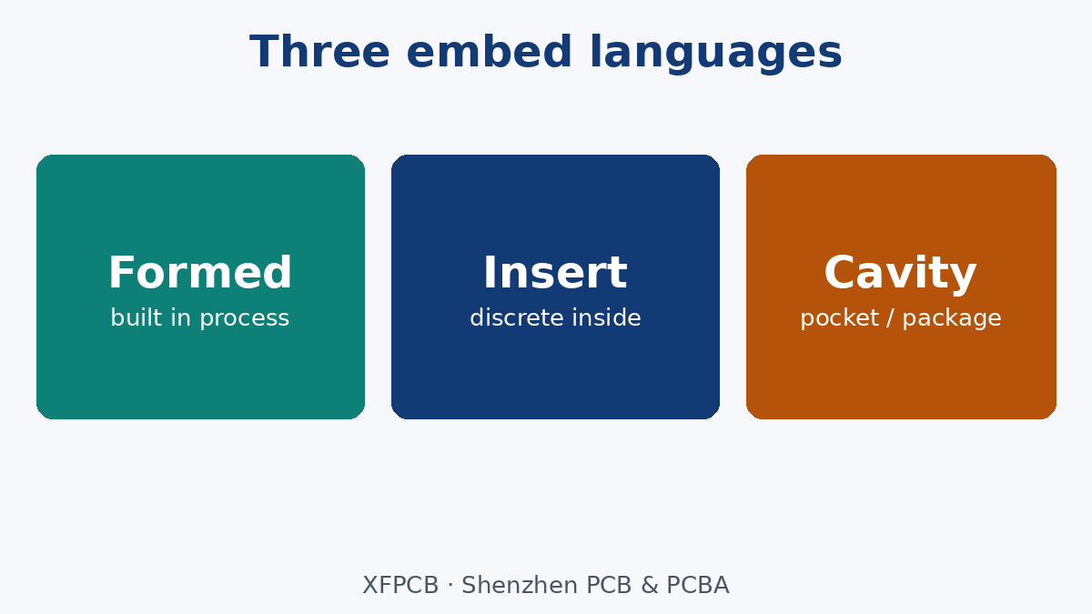
Three paths—pick one language on the drawing
| Path | What it is | Typical fab ask |
|---|---|---|
| Formed | Function made in process (resistive foil, planar capacitance, spiral inductors) | Material callouts, etch/trim rules, tolerance class |
| Inserted | Discrete SMT (or bare die) placed in an inner opening, then laminated | Part height, cavity clearance, attach method, interconnect |
| Cavity / package | Machined or built-up pocket for a module or shield can seating | Depth datum, floor finish, plating intent, keep-outs |
Using “embedded capacitor” for both a thin dielectric plane and a buried 0402 is how CAM opens three EQs. Name the path.
Fab constraints that quietly kill the RFQ
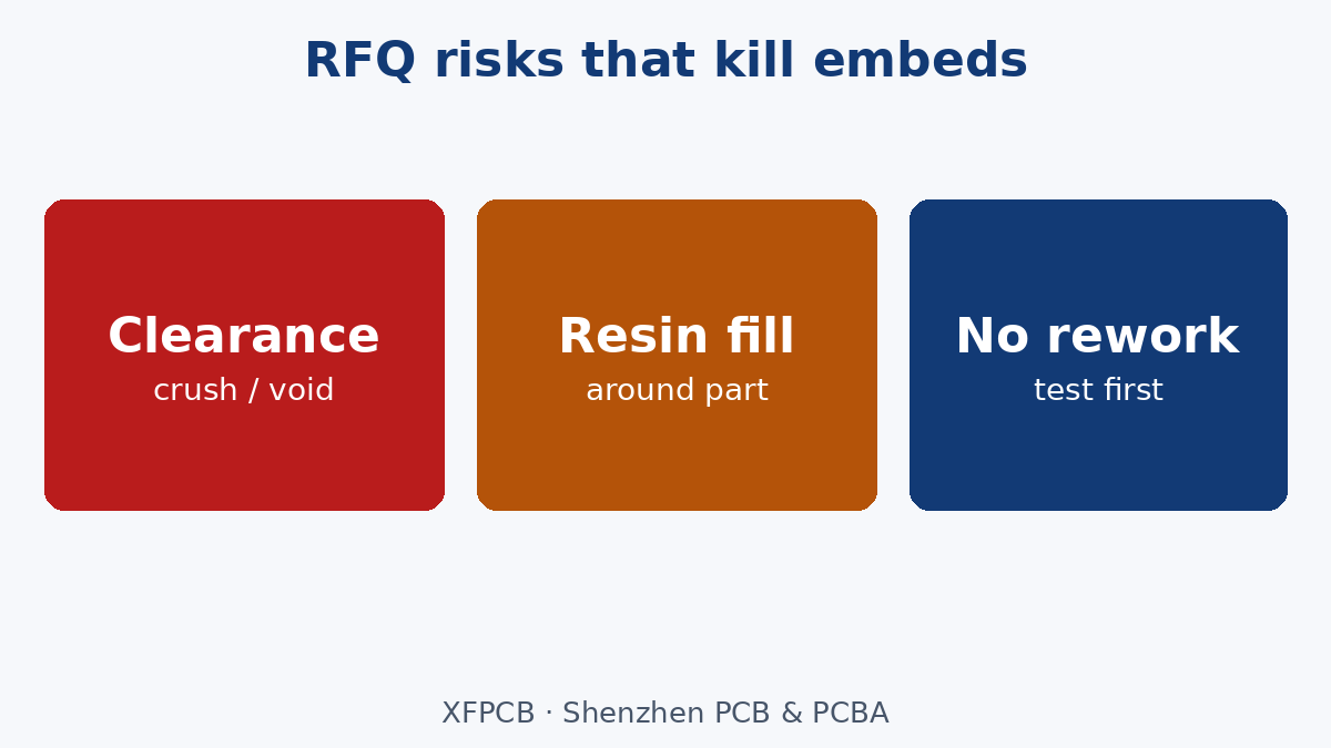
Thickness and flatness. Inserted parts need a cavity or relief that matches package height plus adhesive/underfill. Too shallow → crush or resin void; too deep → resin starve and void at the lid. Call out finished board thickness and cavity depth from a named datum—not only a 3D model.
Registration. Inner openings must land relative to pads and cores after press. High layer counts raise scale risk; treat cavity and insert windows like critical drill features on the fab note.
Resin fill and voids. Prepreg must fill around the part without crushing terminals. Ask how the plant fills (prepreg stack, resin-coated foil, adhesive film)—and whether voids are inspected by microsection or X-ray on FAI.
Interconnect. How does the buried part join the circuit—via to pad, plated pocket, wire bond, or solder before press? Each path has its own cleanliness and thermal limit. Do not leave “connect somehow” to the fab.
Test and rework. Buried failures are rarely reworkable. Freeze in-circuit / flying-probe access, coupon strategy, and scrap disposition before volume. If you need field replaceability, keep that function on the surface.
Active vs passive—different risk stories
Passives (formed or inserted) usually chase density, parasitics, or matching. Formed resistors need tolerance and drift ownership (trim? accept window?). Planar capacitance needs dielectric thickness control—tie to stack notes, not a marketing “embedded cap” checkbox.
Actives (die or packaged IC inside the stack) add yield, known-good-die, thermal path, and moisture sensitivity inside the laminate. Treat them as a module build with a separate SOW if the plant is not already qualified on that flow. Do not bury an unproven BGA “to save height” on a first China prototype without a failure plan.
Copper coins for heat are a different embed class—thermal path and DFM live in their own article. Do not merge coin RFQs with resistor-film or cavity-IC packages on one vague “embedded” line.
Buyer checklist for the fab note / EQ
- Path named: formed / insert / cavity (and copper-coin only if that is truly the ask).
- Part or material identity, height, and keep-outs.
- Cavity depth datum and floor finish (plated? solderable? bare laminate?).
- Lamination / fill method expectations for FAI.
- Electrical access for test; scrap vs rework policy.
- Who owns tolerance on formed R/C values.
For stack and process context see PCB Fabrication Process and the HDI PCB page when microvias share the same density drive. Complex layer builds start from the Multilayer PCB Guide.
What we are not claiming
No invented density “% smaller” claims, no universal cavity-depth table, no statement that every China fab runs buried die, and no overlap with copper-coin thermal or printed-resistor process deep dives. Choose the embed path deliberately—then put clearance, fill, interconnect, and test limits on the note so the quote describes a buildable board.