
Card-edge reliability fails in procurement long before it fails in the connector. Capability pages list hard-gold process; this article is the buyer RFQ checklist—bevel, hard gold versus ENIG on solder pads, plating mask, and wear evidence—so the fab note matches the mating connector.
Hard gold on fingers is not ENIG on SMT pads
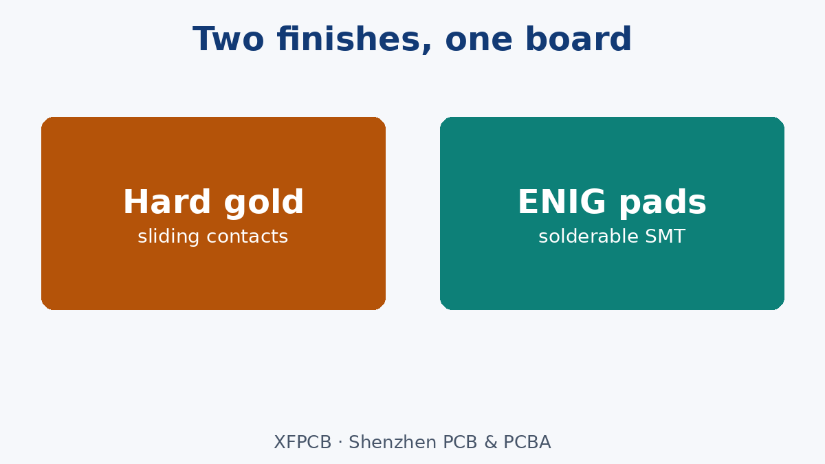
Electrolytic hard gold over nickel on the finger array is for sliding wear. ENIG on component pads is for solderability and flatness. Many boards need both: selective hard gold on the edge, ENIG (or another finish) elsewhere. Writing “gold finish” once on the RFQ invites the wrong stack on the contacts.
Freeze on the note:
- Selective electrolytic hard gold on card-edge contacts only.
- Gold and nickel thickness fields filled from the connector / OEM spec—not a blog default.
- Finish for the rest of the board named separately.
Bevel is a geometry callout, not an angle slogan
Bevel guides insertion and protects springs. Specify more than “45°”:
- Finished board thickness.
- Bevel angle, depth, and remaining edge thickness.
- Where the bevel starts relative to the effective mating length.
- Single- vs double-sided bevel.
Over-bevel cuts into usable gold, exposes copper or inner layers, and leaves the spring on a slope. Under-bevel raises insertion force and scrapes square edges. Match the connector entry drawing.
Plating mask, bus bars, and lead removal
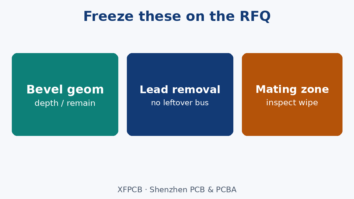
Hard gold needs an electrolytic path. Plants use plating bars, ties, and leads that must disappear from the finished part—by route, bevel, or secondary etch. Incomplete lead removal means shorts or exposed copper at the edge. On the RFQ:
- Call out long/short or segmented fingers if sequencing matters (ground-first, power-first)—with lengths and nets.
- Require inspection that plating leads are gone and no copper shows in the mating wipe.
- Keep solder mask and silkscreen out of the mating area; ink debris kills connectors.
Inner copper pullback near the bevel prevents exposing planes. That is a fab-note keep-out, not a reason to delete the entire reference under the edge if SI needs it—balance both.
Wear and inspection that belong on FAI
- Scratches that expose nickel or copper in the mating zone ≠ cosmetic marks outside the wipe.
- Thickness reports on gold/nickel when the class demands them.
- Outline, keying notches, and bevel dimensions checked against the connector.
- Cleanliness: fingerprints and residues are contact resistance.
Protective packaging is part of the PO if fingers ship exposed.
Where this sits vs capability pages
Product and capability pages describe what a plant can build. This checklist is what you must write so two fabs quote the same edge. For process context see PCB Fabrication Process. Connector-heavy industrial builds often sit under Industrial Control. Order file discipline: Manufacturing Files.
What we are not claiming
No universal gold microinch table, no “ENIG is fine for 10k insertions” claim, no ITAR pitch, and no duplicate of the gold-finger capability brochure. Fill bevel, selective hard gold, mask keep-outs, and mating-zone inspection on the RFQ—then the edge that ships matches the connector you bought.