
Low-cost PCB lists that publish dollar tables and “save 40%” slogans go stale the week copper, freight, or capacity moves. This is a 2026 cost-trap map from a China factory desk: what quietly inflates quotes even when the unit price looks friendly. No invented prices, no supplier rankings, no fake percent savings.
Start from landed cost, not the line-item tease
A usable comparison is bare-board process + test + packing + freight/duties + the probability of a respin. Skipping flying-probe on a dense prototype to “save” often buys a respinned week. Rush premiums and non-standard cosmetics are still the fastest ways to multiply a standard-spec job.
Panel utilization
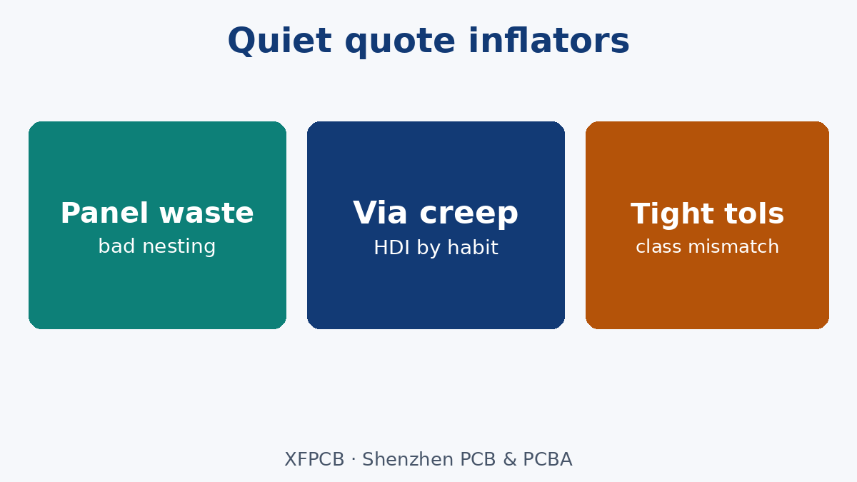
Small oddly shaped boards that waste panel area pay for copper and process time you never assemble. Ask:
- Can the outline nest efficiently on the fab’s production panel?
- Are rails, coupons, and fiducials shared or duplicated per piece?
- Is customer panelization frozen, or will the plant re-panel (and change SMT depanel method)?
Good nesting is free DFM; bad outlines are a silent tax.
Layer and via choices
Each added layer is another press, drill, and plate cycle. Blind/buried, via-in-pad (plated shut), back-drill, and microvia stacks move the job out of commodity pricing—even if the schematic “only needed one extra net.” Before you add HDI for convenience:
- Can the net escape with through-vias and a sane BGA fanout?
- Are via sizes inside the quoted mechanical window, or did CAD push micro-drills by habit?
- Is aspect ratio forcing sequential laminate you did not budget?
Finish, mask, and cosmetics
ENIG, hard gold, and specialty finishes earn their keep on fine-pitch, shelf life, or wear contacts. HASL-family finishes remain the workhorse for many through-hole and coarse SMT jobs. Non-green masks, ultra-matte cosmetics, and dense silkscreen rarely improve function and often add process risk. Choose finish for package and reliability, not brochure shine.
Tolerances that quietly inflate quotes
- Hole and outline tolerances tighter than the class needs.
- Impedance on every net “just in case.”
- Copper balance / plating thickness windows copied from aerospace onto a consumer UI board.
- Controlled depth / cavity features that are really mechanical preferences.
Tighten only where function or connector mating demands it—and put that reason on the fab note so EQ does not guess.
Honest China-factory framing
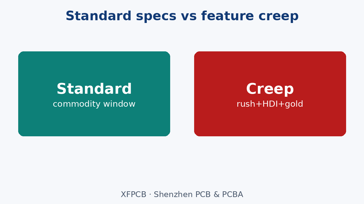
Overseas volume fabs win on standard specs repeated with clear files. They lose money—and you lose schedule—when the RFQ mixes rush, exotic finish, HDI, and undefined test. Local quick-turn still wins for same-day iteration and export-control venue; that is a region gate, not a morality play. We do not claim ITAR/DDTC capability.
See Low Cost PCB for the service frame, Quick Turn PCB when schedule is the scarce resource, and How to Place an Order for file expectations.
What we are not claiming
No price tables, no “top 10 fabs,” no “save X% with green mask” invented math, and no lead-time guarantees. Kill the traps—panel waste, via creep, finish vanity, and tolerance theater—so the 2026 quote you compare is the job you actually intend to build.