
Ground-plane advice that stops at “pour more copper” dies in CAM. High-speed return-path theory matters, but overseas hardware teams also need what survives fab: continuous planes, intentional splits, stitching vias, and copper balance so etch and plate do not warp the panel. This is that fab-tied view—not a generic SI textbook.
Continuity is a stackup and a keep-out problem
A reference plane only works if high-speed traces see unbroken copper under their path. Anti-pads, connector cutouts, and dense via fields punch holes; that is normal. Accidental slots from “isolation moats,” logo cutouts in the plane, or split pours under differential pairs are not. On the fab note / stackup:
- Name which layers are solid GND (and which are power).
- Call out no-route / no-split zones under critical interfaces.
- Treat large plane voids as design features that need review—not surprises in Gerber.
Two-layer boards rarely get a true internal plane; a fragmented pour is not the same as a dedicated GND layer on four-layer and up. Choose layer count for the reference you need.
Splits: only with a return plan
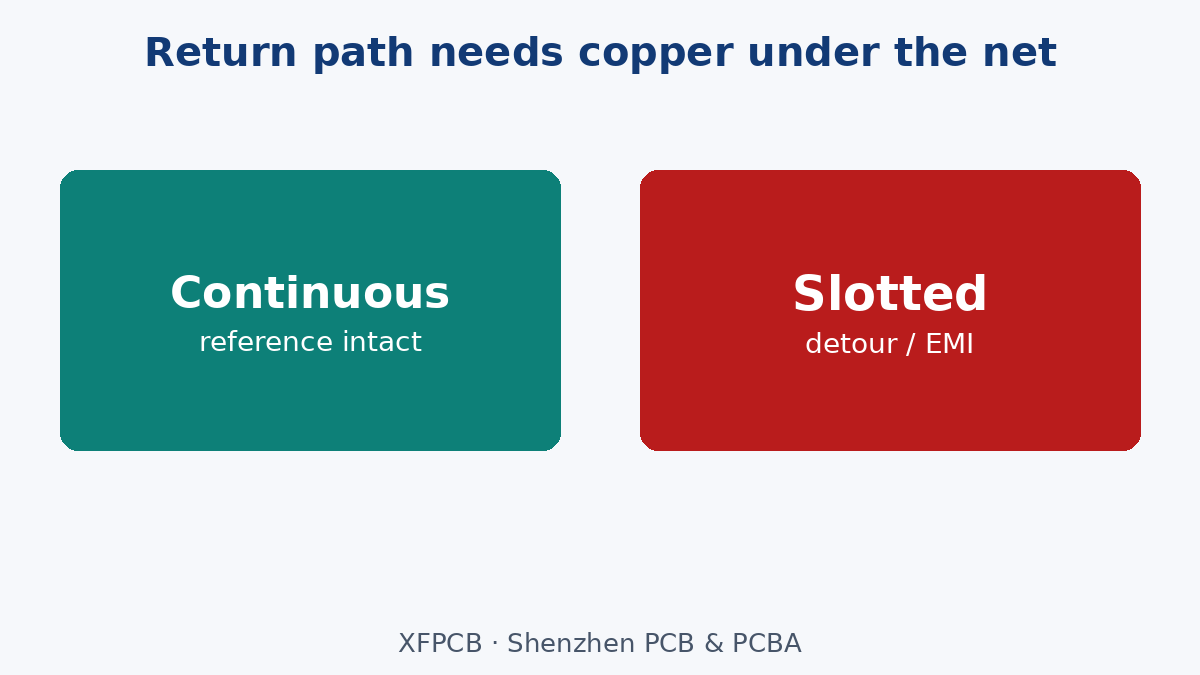
Splitting GND for analog/digital or chassis/signal can help—or force return current into long detours. If you split:
- Document where domains join (single-point, bridge, or component).
- Keep each class of signal over its own reference.
- Do not let a shield can or metal stiffener accidentally short domains you meant to separate (see EMI callout post).
Power-plane splits for voltage rails are common; do not copy that habit onto GND without an EMC owner.
Stitching vias and copper balance
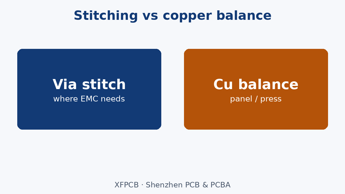
Via stitching along shield fences, board edges, or around connectors lowers impedance between planes and seams. It also:
- Steals routing channels.
- Creates swiss-cheese copper that changes etch loading.
- Adds drill count (cost and registration risk on dense boards).
Put stitch pitch intent on the drawing when EMC needs it; do not spray vias “for luck.”
Copper balance across the panel and between layers matters to the fab: uneven copper warps press-out, skews impedance, and complicates plating. Cross-hatch sparingly and knowingly—hatch is not free EMI magic and can hurt return continuity. Ask the plant if your copper distribution needs thieving on unused areas; that is a fab note conversation, not a layout afterthought.
Return path vs “slotting copper for isolation”
Slotting a plane to “keep noise out” often creates the antenna. Prefer component placement and continuous reference; use splits only with documented bridges. When a slot is unavoidable (connector, module cutout), provide a defined return around it—or accept the SI/EMI EQ.
What to put on fab / stack notes
- GND and power layer assignment in the stackup table.
- Impedance references (which plane each coupon uses).
- Keep-outs where planes must stay solid.
- Stitch via rules only where functional.
- Copper balance / thieving ownership if the plant requires it.
See 4-Layer PCB and Multilayer PCB Guide for layer-count context, and Impedance Control PCB when the plane is also an impedance reference.
What we are not claiming
No universal stitch-pitch millimeter table, no claim that cross-hatch always improves EMC, no invented PDN impedance curves, and no “always split AGND/DGND” rule. Design the return path—then freeze continuity, splits, stitching, and copper balance so the plane that fabs is the plane you simulated.