
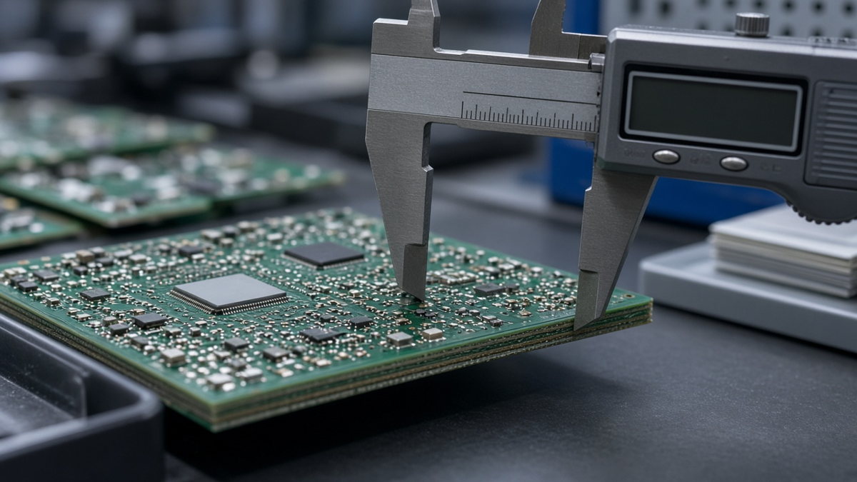
Finished board thickness is rarely chosen because someone prefers a round millimetre. It is chosen because something else already owns the number: a card-edge connector slot, a ZIF/FPC mate window, a heatsink stand-off stack, a chassis rail, a rigid-flex step height, or a dielectric height that impedance modeling already spent. When those owners disagree—and the RFQ still says only “1.6 mm ±10%”—CAM will hit a thickness, the FA caliper will read another story, and SMT will discover warp or unsupported thin panels the thickness line never mentioned.
This article is not a catalog of 0.4–3.2 mm standards. Those lists exist elsewhere on the site. It is the buyer and process view of finished thickness as a controlling constraint: how conflicts arise, what “tolerance” must actually specify, where thickness is measured, how thin and thick boards fail differently at fab and assembly, and what to freeze in an RFQ thickness block before quotes pretend to be comparable.
Stack construction detail (cores, prepreg, impedance layers as a fab document) belongs in PCB stack-up as a fab document. How prepreg becomes pressed dielectric thickness belongs in prepreg selection and pressed thickness. Copper ounces as a capability—not overall board height—belong in copper thickness capabilities. Here the focus is the finished number on the PO and the fights it loses when left vague.
Finished thickness is a system output, not a dropdown
What arrives in the carton is roughly:
cores + pressed prepregs + copper (including plating) + solder mask / surface finish contributions at the measure point
Buyers often mean “dielectric + copper like the CAD stack viewer.” Fabs often mean “what the micrometer reads after process at an agreed location.” Those are not the same contract unless you write them as one.
Three different “thickness” ideas collide on one RFQ line:
| Phrase on RFQ | What people think | What plants often build to | Conflict if undefined |
|---|---|---|---|
| Nominal finished thickness | Enclosure / connector fit | Overall after process | Mask and plating push high |
| Dielectric / core height for impedance | Modelled stack heights | Pressed PP + core as run | Nominal mm met with wrong dielectric split |
| Copper weight | Current / thermal | Oz on foil / plate-up | Heavy copper raises finished height and drill stress |
If the PO freezes only the overall millimetre, CAM may satisfy the caliper by changing prepreg count or resin content while your impedance-controlled layers move. If the PO freezes only impedance dielectrics, the connector slot may go out of tolerance. Controlling constraint means you name which requirement wins when both cannot be perfect, and you give CAM an allowed construction window—not a single orphaned number.
Constraint owners that silently set the millimetre
Before you “pick a thickness,” list what already picked it for you.
Connector and card-edge Z
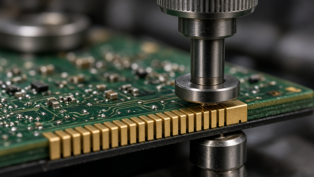
Edge connectors, backplane slots, and many board-to-board systems assume a finished thickness band. Too thick: will not enter or will damage the housing. Too thin: contact force collapses, intermittents under vibration. The datasheet window is the owner; your stack is the servant. Call out the connector PN and the thickness band on the mechanical drawing, not only in an email.
Heatsink, chassis, and standoff stacks
Thermal pads, extruded sinks, and sheet-metal gaps add a second Z budget. A board that grew after plating and mask can crush a gap pad or leave a sink floating. Conversely, a thin board under a heavy sink needs support so the sink does not become a bending brake.
Flex-to-rigid and stiffener steps
Rigid-flex and stiffened flex create local height steps. The rigid finished thickness and the flex finished thickness are different controlling numbers. Do not RFQ one overall thickness for a construction that has two mechanical faces. Name each zone.
Panel and SMT process
Thin boards flex in print and reflow; thick boards fight depaneling and raise drill aspect ratio. Process risk can veto a mechanically “perfect” connector thickness if the panel cannot be supported. Thickness is then a three-way negotiation: fit, SI, and line capability.
Impedance dielectric vs overall height
High-speed layers care about dielectric distance and foil type. Overall height is the sum. When layer count, copper weight, and impedance targets fill the millimetre budget, something gives: overall height, copper weight, or impedance geometry. Make the give intentional.
Conflict matrix: what to freeze when two owners fight
| Conflict | Typical symptom | Buyer freeze that helps | Weak freeze |
|---|---|---|---|
| Connector band vs impedance stack | Slot fit OK, SI fails—or SI OK, will not mate | Primary owner named; allowed overall band; dielectric heights for impedance layers locked in stack PDF | “1.6 mm, impedance controlled” with no stack |
| Heavy copper vs overall height | Caliper high; drill/aspect issues | Copper oz per layer + max finished; plate-up assumption | Copper “as needed for current” |
| Thin overall vs SMT warp/support | Paste smear, tombstone, BGA corner lift | Finished min + panel support / carrier note | “0.8 mm for weight” only |
| Thick overall vs small vias | Thin plating in barrels | Min finished + min drill / aspect rule agreed | Thickness without hole chart |
| Mask-included measure vs bare laminate habit | FA “too thick” arguments | Measure method: with/without mask, location | ±10% with no measure point |
| Zone A vs zone B (rigid-flex) | One zone fit, other fails | Per-zone finished thickness | Single mm for whole part |
Primary owner language example (adapt, do not copy as legal boilerplate): “Card-edge finished thickness band per connector PN xxx is the primary mechanical constraint. Impedance layers L3–L4 shall keep dielectric construction per stack Rev B. If conflict, stop and EQ—do not silently thin impedance dielectrics to hit overall mm.”
Tolerance that can be measured (and argued)
“±10%” without a method is how FA meetings become philosophy. Thickness tolerance needs at least:
- Nominal (and units).
- Band ( asymmetric bands are allowed if the connector is asymmetric in risk—too-thick may be worse than too-thin).
- Measure points (edge, near connector, away from copper pour extremes, count of points).
- What is included (solder mask yes/no; selective thick gold areas excluded or not).
- Instrument / method class (micrometer / calibrated stack; agree before FA).
- When (after fab, before assembly; after assembly only if that is the real fit condition—rare and messy).
Plating and mask almost always push up. If your nominal was modeled as dielectric+copper only, the finished part will read high unless the stack was built with that allowance or the measure excludes mask by agreement. Write the inclusion rule. Do not invent a universal plating/mask add-on in the blog and treat it as factory law—confirm with the stack and the plant.
Coupon vs product: impedance coupons prove dielectric intent; they do not automatically prove connector-edge finished thickness. If fit is the primary owner, measure the product at the mate edge on FA, not only coupon stacks.
Thin-board failure modes (fab and SMT)
Thin finished boards (often sub-1.0 mm class, product-dependent) fail in patterns thickness catalogs understate:
Fab
- Handling dings and corner fractures before they ever see solder.
- Panel warp and bow that pass a center reading but fail edge flatness.
- Breakout and registration sensitivity when cores are thin.
- Inconsistent pressed thickness if PP count is minimal and resin flow has nowhere to “average.”
SMT / assembly
- Board flex under squeegee → uneven paste (support map becomes mandatory).
- Reflow trampoline under heavy parts.
- Connector insertion that bends the board instead of the contacts.
- Depanel stress that cracks ceramics near mouse bites.
RFQ / traveler callouts for thin controlling thickness:

- Panelization and support expectations (carrier, rails, vacuum).
- Depanel method preference when ceramics sit near edges.
- Explicit finished min (not only nominal) if flex under load is the fear.
- Flatness / warp criteria tied to the thin construction—see warped PCB root cause when you need fab-vs-assembly diagnosis depth.
Thick-board failure modes (fab and SMT)
Thick finished boards (often ≥2.0 mm class, or high layer count pressed tall) fail differently:
Fab
- Drill aspect ratio: deep small holes plate poorly if the thickness/drill pair was not agreed.
- Longer drill time, more bit wear, higher risk of smear if desmear is not matched.
- Lamination void risk in dense copper if fill is wrong—thickness target met with sick internals.
- Weight and routing stress on panels.
SMT / assembly
- Heat sinking into the board → profile needs more care for small parts on thick copper/thick dielectric.
- Harder connector press-fit if used; mechanical fixtures must match.
- Depanel: thicker boards need different routing/V-score parameters; forced thin-board habits crack.
RFQ callouts for thick controlling thickness:
- Finished max if enclosure crush is the risk.
- Hole size / aspect agreement with the thickness.
- Copper weight honesty (copper thickness capabilities) so plate-up does not silently grow Z.
- Press-fit or heavy connector notes so the plant does not treat it like a 1.6 mm consumer board.
Where thickness fights the stack document
A good stack PDF locks cores, prepreg styles, and impedance dielectrics. A good thickness RFQ locks finished Z and measure rules. They must cross-reference:
- Stack Rev X is authoritative for dielectric constructions on impedance layers.
- Drawing note Y is authoritative for finished thickness band and measure method.
- If CAM cannot satisfy both, EQ is mandatory—no silent prepreg substitution to chase the caliper.
Pressed thickness reality for prepreg is why “paper” stacks miss finished mm: resin flows, copper islands displace volume, and the press recipe matters. That physics sits in the prepreg pressed-thickness guide; the buyer action here is simpler: do not treat CAD viewer sum as FA caliper truth without plant confirmation of pressed constructions.
RFQ thickness block (paste and fill)
Require every bidder to mirror this block. Quotes that only say “1.6 mm FR-4” are not thickness contracts.
| Field | What to write |
|---|---|
| Primary owner | Connector PN / enclosure gap / impedance / other — one primary |
| Nominal finished thickness | Value + unit |
| Allowed band | Min–max or +/– ; note if asymmetric |
| Measure points | Locations, count, exclude zones (gold fingers thick plate, etc.) |
| Inclusions | Mask yes/no; finish contribution handling |
| Per-zone thicknesses | Rigid / flex / stiffener zones if applicable |
| Stack reference | Stack PDF rev; impedance layers that must not be sacrificed |
| Copper weights | Per layer or class; plate-up expectation if critical to Z |
| Thin-board process notes | Support / carrier / depanel if below your plant comfort |
| Thick-board process notes | Aspect ratio / drill min if above comfort |
| Warp / flatness | Criteria or pointer to drawing; stage of measure |
| FA evidence | Caliper log at named points + photo optional |
| Conflict rule | EQ if stack and finished Z disagree — no silent trade |
Ask the quote to restate primary owner, band, and measure inclusions. If two plants restate different inclusions, they are not bidding the same board.
Decision table: freeze overall, freeze dielectrics, or freeze both
| Situation | Freeze overall finished | Freeze impedance dielectrics | Freeze both + conflict rule |
|---|---|---|---|
| Card-edge / slot mate is critical | Required | If SI present, yes | Preferred |
| Pure digital, no tight Z mate, SI critical | Band only (enclosure) | Required | Yes if enclosure exists |
| Wearable thin + SI | Min overall + support notes | Required | Yes |
| Power thick + heavy copper | Max overall + aspect | As needed | Yes |
| Rigid-flex | Per zone | Per rigid SI zones | Yes |
| Prototype learning spin | Soft band OK | Soft OK | Still name measure habit |
Default for overseas production RFQs with any mate or chassis fit: both + conflict rule. Overall-only is how SI dies quietly. Dielectric-only is how connectors refuse to latch.
Failure symptoms → thickness contract miss
| What you see | Likely miss | First corrective ask |
|---|---|---|
| Will not enter connector | Finished high or measure excluded mask differently than design | Measure method + band vs PN; plating/mask inclusion |
| Intermittent card edge | Finished low / warped edge | Band min + edge flatness + measure at mate |
| Impedance fail, caliper OK | Dielectrics sacrificed to hit overall | Stack lock; conflict rule |
| Caliper fail, SI OK | Nominal modeled without mask/plate | Inclusion rule; retarget nominal |
| Thin panel SMT defects | No support plan for thin finished | Carrier / rails; warp criteria |
| Barrel plating issues on thick | Aspect vs thickness not agreed | Drill chart vs finished max |
| Heatsink gap wrong | Post-mask thickness ignored in MCAD | Measure with mask; MCAD update |
| Rigid-flex step interference | Single thickness for two zones | Per-zone finished callouts |
What to decide before the next thickness line on the PO
Do not start from a preferred catalog millimetre. Work this list:
- Who owns the number? Connector, chassis, heatsink, flex step, or SI dielectric—name one primary and any hard secondaries.
- What band is real? Datasheet window or MCAD gap, including whether too-thick or too-thin hurts more.
- What does FA measure? Points, inclusions, instrument class, timing.
- What must the stack keep anyway? Impedance dielectric constructions and copper weights that cannot be traded for caliper convenience.
- What process notes follow thin or thick? Support, depanel, aspect ratio, carrier.
- What happens on conflict? Written EQ—not silent CAM artistry.
- Does every bidder’s quote restate the block? If not, re-bid.
Fill the RFQ thickness block until those answers are boringly explicit. Catalog tables do not protect fit, SI, or SMT yield. A finished-thickness contract—with owners, measure rules, and a conflict stop—does. When the primary owner changes (new connector, new sink, new layer count), reopen the block on purpose; do not inherit last product’s 1.6 mm habit onto a different Z budget.